Showing Spotlights 121 - 128 of 338 in category All (newest first):
 Motivated by the outstanding performance of graphene, graphene-like 2D materials have been intensively investigated, such as topological insulators, transition metal dichalcogenides (TMDs) and black phosphorous. Recently, 2D titanium disulfide, a typical TMD, is found to have strong light absorption properties from visible to infrared region, which is highly attractive for applications in nonlinear photonics. Researchers have fabricated a novel saturable absorber device is successfully fabricated based on 2D TiS2 nanosheets for ultrashort pulse generation and all-optical thresholding at the communication band.
Dec 27th, 2018
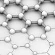
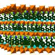 Due to the unique physical and chemical characteristics, such as good electrical conductivity, low weight, large surface areas, high electrochemical activity, and facile doping of heteroatoms or inorganic species, there are increasing demands of fabricating two-dimensional (2D) porous carbon for lithium-ion batteries, supercapacitors, electrochemical catalysts and many other emerged applications in energy storage and conversion. Researchers now have developed a fast, scalable, and eco-friendly active-salt-templating strategy to engineer different types of 2D porous carbons.
Dec 21st, 2018
 One of the most pervasive reliability problems facing the computer chip industry is ESD (electrostatic discharging) failure caused by the rapid, spontaneous transfer of electrostatic charge induced by a high electrostatic field. A novel above-IC graphene based nanoelectromechanical system (NEMS) switch structure for on-chip ESD protection utilizes the unique properties of graphene. This switch is a two-terminal device with a vacuum gap between a conducting substrate at the bottom and a suspended graphene membrane on top serving as the discharging path.
Dec 4th, 2018
 Scientists report the experimental results of studying the response characteristics in a millimeter wave band whispering gallery mode sapphire resonator to single-layer graphene at different distances of graphene from the resonator. They found that the evanescent field of the resonance system is extremely sensitive to the environment, surrounding materials and disk coatings. A series of experiments showed that such whispering gallery mode resonance can be used to detect the conductivity and thickness of the materials deposited on top and/or can even be used for advanced biosensing.
Nov 21st, 2018
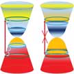
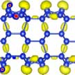
 In recent years, black-phosphorus-analogue (BPA) two-dimensional materials have been demonstrated to exhibit promising optoelectronic performances and distinguished ambient stabilities, holding great promise in practical applications. In new work, researchers demonstrated that ultra-small 2D beta-lead oxide quantum dots showed fast carrier dynamics and significantly high photocurrent density and excellent ambient stability. These findings hold great potential for high-performance BPA-based optoelectronic devices.
Nov 6th, 2018
 Researchers investigated the thermal conductivity and thermal diffusivity of epoxy composites with high loading fractions of graphene and h-BN fillers. They found that the graphene fillers outperformed boron nitride fillers in terms of thermal conductivity enhancement. The surprising finding is that, in the high loading composites with quasi-2D fillers, the apparent cross-plane thermal conductivity of the fillers can be the limiting factor for heat conduction. These results are important for developing the next generation of the thermal interface materials.
Oct 30th, 2018
 In the past few years, monolayer and multilayer silicenes have been successfully grown on various metal substrates. Unfortunately, silicene on metal substrate generally exhibits metallic or semi-metallic character without a bandgap, and thus cannot be used as adsorption layer of photovoltaic materials. A new comprehensive investigation of multilayer silicene by means of ab initio swarm-intelligence structure-searching method predicts that tri-layer silicene is an ideal candidate for high-efficiency photovoltaic absorbers.
Oct 15th, 2018
 A new study on worldwide graphene production shows unequivocally that the quality of the graphene produced in the world today is rather poor, not optimal for most applications, and most companies are producing graphite microplatelets. This is possibly the main reason for the slow development of graphene applications, which usually require a customized solution in terms of graphene properties. A conclusion that sounds even more damming is that this extensive study of graphene production worldwide indicates that there is almost no high quality graphene, as defined by ISO, in the market yet.
Oct 9th, 2018
 Subscribe to our Nanotechnology Spotlight feed