Nanotechnology Spotlight – Latest Articles
 Subscribe to our Nanotechnology Spotlight feed
Showing Spotlights 1849 - 1856 of 3579 in category All (newest first):
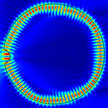
Chemically enhanced 2D material makes excellent tunable nanoscale light source
Molybdenum disulfide's (MoS2) semiconducting ability, strong light-matter interaction and similarity to the carbon-based graphene makes it of interest to scientists as a viable alternative to graphene in the manufacture of electronics, particularly photoelectronics. In particular, MoS2 has excellent optical properties when deposited as a single, atom-thick layer - unlike graphene, it emits light when excited; albeit relatively poorly. In order to realize the potential of atomically thin MoS2 as a nanoscale active material in a light source, a considerable enhancement of its emission efficiency is necessary.
March 12, 2015
Has nanomedicine lived up to its promise?
Historically, the approval of Doxil as the very first nanotherapeutic product in 1995 is generally regarded as the dawn of nanomedicine for human use. Although numerous products classified as nanomedicine products have indeed appeared over the past decade, such products have not exactly revolutionized treatment paradigms as envisaged earlier. In particular no molecular machine or nanorobot has yet entered clinical trials, although research in these areas is picking up pace.
March 10, 2015
A thermionic energy converter using single-layer graphene
Heat energy can be converted into electricity with very high efficiency through a temperature-induced electron flow process known as thermionic emission. Thermionic energy converters have been used with different heat sources, all of them requiring operation at high temperatures above 1500 K. A new study indicates that heat temperature can be lowered by an order of magnitude if using graphene as hot cathode. The findings indicate that a graphene-based cathode thermionic converter operating at 900 K could reach an efficiency of 45%.
March 5, 2015

Lower cost, roll-to-roll production of carbon nanotube based supercapacitors
Supercapacitors offer an alternative source of energy to replace rechargeable batteries for various applications, such as mobile electronics and electric vehicles. Among the various types of supercapacitors, carbon nanotube based devices have shown an order of magnitude higher performance in terms of energy and power densities. The bottleneck for transferring this technology to the marketplace, however, is the lack of efficient and scalable nanomanufacturing methods. Researchers have now developed a new scalable method to to directly spraycoat CNT-based supercapacitor electrodes.
March 3, 2015
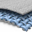
On route to self-powered smart suits
Energy-scavenging fabrics based on nano-sized generators that have piezoelectric properties could eventually lead to wearable 'smart' clothes that can power integrated electronics and sensors through ordinary body movements. Researchers have now demonstrated a new type of fully flexible, very robust and wearable triboelectric nanogenerator with high power-generating performance and mechanical robustness. This was achieved by applying a bottom-up nanostructuring approach where a silver-coated textile and polydimethylsiloxane (PDMS) nanopatterns based on ZnO nanorod arrays were used as active triboelectric materials.
February 25, 2015
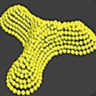
Assembling nanoparticles into 3D structures with one microdroplet
Existing fabrication techniques for 3D microstructures usually suffer from complicated equipment, time-consuming processes, and insufficient controllability on precise structures. Constructing controllable 3D self-assembly microstructure in a simple and convenient way is still a challenge. In new work, researchers propose a facile strategy to directly assemble nanoparticles into controllable 3D structures from one microdroplet based on 0D hydrophilic pinning pattern.
February 24, 2015
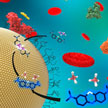
A simple test kit for the detection of nanoparticles
Meeting the need for a reliable, sensitive, and accurate methodology for the detection of nanoparticles in complex samples, using low-cost and portable instrumentation, scientists have developed a novel methodology to quickly screen for the presence and reactivity of nanoparticles in commercial, environmental, and biological samples. A colorimetric assay - similar to a swimming pool test kit - tests for the presence or absence of nanoparticles in biological and environmental relevant samples with sufficient sensitivity at part per billion concentration levels.
February 20, 2015
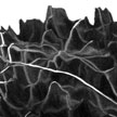
Non-destructive subsurface imaging of carbon nanotubes in polymer composites
Researchers report a non-destructive and high throughput 3D imaging of carbon nanotubes (CNTs) embedded in polymer matrix via Scanning Electron Microscopy (SEM). While have been several open questions remaining for SEM subsurface imaging of CNTs, this new findings clarify these issues and help establish SEM subsurface imaging as a useful and facile method to provide quantitative 3D information on CNT dispersions in polymer composites.
February 18, 2015