Nanotechnology Spotlight – Latest Articles
 Subscribe to our Nanotechnology Spotlight feed
Showing Spotlights 2121 - 2128 of 3577 in category All (newest first):

Does the EU's chemical regulation sufficiently address nanotechnology risks?
The European Commission acknowledges that nanomaterials are revolutionary materials and that important challenges exist in regard to hazard and exposure assessments. Yet, they conclude that current risk-assessment methods are applicable to nanomaterials. Scientists argue that significant changes to REACH and the accompanying annexes are required to answer the call made by the public, downstream users and progressive businesses for clearer and more definite regulatory rules specific to nanomaterials.
May 28, 2013

Nanotechnology in sports equipment: The game changer
The degree of competitiveness in sports has been remarkably impacted by nanotechnology like any other innovative idea in materials science. Within the niche of sport equipments, nanotechnology offers a number of advantages and immense potential to improve sporting equipments making athletes safer, comfortble and more agile than ever. Baseball bats, tennis and badminton racquets, hockey sticks, racing bicycles, golf balls/clubs, skis, fly-fishing rods, archery arrows, etc. are some of the sporting equipments, whose performance and durability are being improved with the help of nanotechnology. Nanomaterials such as carbon nanotubes, silica nanoparticles, nanoclays fullerenes, etc. are being incorporated into various sports equipment to improve the performance of athletes as well as equipments.
May 27, 2013

A pH-responsive nanoscale vaccine with tailored immune responses
Nanomaterials hold promise as synthetic vaccines. They have the ability to deliver cargo to specific immune cells and modulate the resulting immune response. Compared to natural vaccine vectors, including engineered viruses or attenuated pathogens, synthetic nanoscale vaccines are safer, more controlled, and have the potential to be more effective. Nanoscale vaccines may also prevent, or even treat a wider range of diseases, including cancer. Researchers now have developed nanoscale polymer micelles that elicit both humoral and cellular immunity. The constructs could help in the fight against infectious diseases and cancer.
May 24, 2013

Nanothermometers may aid in the treatment of cancer with heat
Nanotechnology is helping to revolutionize cancer hyperthermia - the treatment of cancer with heat. Certain types of nanoparticles, in particular those made of gold or iron oxide, act as transducers that absorb electromagnetic radiation and generate heat. If the nanoparticles are delivered selectively to a tumour, heat can be generated within the tumour tissue by irradiating it with an external energy source. This results in heat-induced cell death within the tumor, sparing the surrounding healthy tissues. Researchers have now developed gold nanoparticles coated with a temperature-sensitive dye. The constructs allow nanoparticle-induced heating to be monitored locally.
May 23, 2013

A nanotechnology use for hemp
Researchers have come up with various electrode materials to improve the performance of supercapacitors, focussing mostly on porous carbon due to its high surface areas, tunable structures, good conductivities, and low cost. Graphene and carbon nanotubes show great potential but are costly. Researchers in Canada have now reported the successful hydrothermal-based synthesis of two-dimensional, yet interconnected, carbon nanosheets with superior electrochemical storage properties comparable to those of state-of-the-art graphene-based electrodes.
May 15, 2013
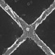
Probing the behavior of single nanomagnets
Ferromagnetic materials exhibit the so-called anomalous Hall effect (AHE), whereby the electrons flowing through the material experience a lateral force pushing them to one side as a result of the material's intrinsic magnetization. Although the AHE has been used in the field on nanotechnology to measure the magnetic behavior of nanoparticles (with sizes larger than 50 nm), nobody so far had tried to separate the signals of the individual particles. Researchers in Germany have now developed a simple technique which allows to measure the magnetic response of single ferromagnetic nanoparticles down to a radius of about 3.3 nm.
May 14, 2013
Unusual behavior of graphene under irradiation: More damage - less noise
The low-frequency 1/f noise is a ubiquitous phenomenon found everywhere from fluctuations of human heart rates to fluctuations of electrical currents in semiconductor devices. An acceptable level of flicker 1/f noise is one of the key metrics that each new material has to pass before it can be used for practical devices. Graphene has shown a great potential for applications in high-frequency communications, analog circuits and sensors. The envisioned applications require a low level of 1/f noise, which contributes to the phase-noise of communication systems and limits the sensor sensitivity. Now, researchers have discovered a unique feature of 1/f noise in graphene, which can help understand its microscopic origin and develop new techniques for noise reduction.
May 10, 2013

Single-molecule nanopore research made easy
Nanopores are an exciting class of single molecule nanosensors. For several years now, nanopore technology has been developed as a biosensor at the single-molecule resolution to detect an array of biomedical molecules, such as DNA, RNA, protein, biotoxin, and various nanopore projects have been funded to develop the next generation of DNA sequencing technology. The sensing principle is based on the resistive pulse technique - molecules are detected as they pass through a single nanopore since during translocation the molecules exclude ions and therefore modulate the current. In new work, researchers have demonstrated the single molecule detection of a wide range of proteins with solid state glass nanopores.
May 9, 2013