Showing Spotlights 369 - 376 of 624 in category All (newest first):
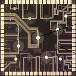
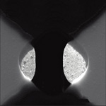 Researchers worldwide are working on fast and low-cost strategies to sequence DNA, that is, to read off the content of our genome. Particularly promising for future genome sequencing are devices that measure single molecules. In this respect, the creation of nanochannels or nanopores in thin membranes has attracted much interest due to the potential to isolate and sense single DNA molecules while they translocate through the highly confined channels. Particularly interesting are techniques that can offer fast and low cost readout of long DNA molecules without the need of DNA labelling or amplification. In very interesting work performed at Imperial College London, researchers have now successfully developed a protocol for the fabrication of a solid state nanopore aligned to a tunneling junction.
Dec 13th, 2010
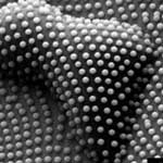 Projection photolithography is mostly limited to flat surfaces. However, many emerging areas of micro- and nanotechnology applications, be it in optics, imaging, sensors or bioengineering, increasingly require the fabrication of microscopic and nanoscopic patterns on nonplanar surfaces. Contact printing and imprinting methods can cope with certain curved surfaces but appear to be restricted to those having a constant magnitude of curvature and a large radius of curvature relative to the arc length at least in one dimension. Researchers have now demonstrated that hexagonal noncontiguously packed (HNCP) colloidal crystals trapped at the air-water interface can be directly transferred onto solid substrates to give HNCP and distorted HNCP patterns. This bottom-up method uses self-assembled nanoparticle arrays and is not limited to flat surfaces at all.
Dec 6th, 2010
 Dip-Pen Nanolithography (DPN) is a scanning probe lithography technique in which the tip of an atomic force microscope (AFM) is used to deliver molecules to a surface, allowing nanostructured surface patterning on scales of under 100 nm. This direct-write technique offers high-resolution patterning capabilities for a number of molecular and biomolecular 'inks' on a variety of substrates, such as metals, semiconductors, and monolayer functionalized surfaces. It's becoming a work-horse tool for the scientist interested in fabricating and studying soft- and hard-matter on the sub-100nm length scale.
Using DPN for fabricating graphene devices has not been previously shown. Researchers at Stanford University have now evaluated DPN as an alternative to conventional electron-beam lithography (EBL) for tailoring such devices.
Dip-Pen Nanolithography (DPN) is a scanning probe lithography technique in which the tip of an atomic force microscope (AFM) is used to deliver molecules to a surface, allowing nanostructured surface patterning on scales of under 100 nm. This direct-write technique offers high-resolution patterning capabilities for a number of molecular and biomolecular 'inks' on a variety of substrates, such as metals, semiconductors, and monolayer functionalized surfaces. It's becoming a work-horse tool for the scientist interested in fabricating and studying soft- and hard-matter on the sub-100nm length scale.
Using DPN for fabricating graphene devices has not been previously shown. Researchers at Stanford University have now evaluated DPN as an alternative to conventional electron-beam lithography (EBL) for tailoring such devices.
Dec 3rd, 2010
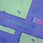
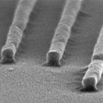
 The workhorse of current nanofabrication processes, electron beam lithography (EBL), has good resolution but has good resolution, it is difficult to precisely control the pattern size at the sub-20 nm scale due to the proximity effect and the large beam spot. A more recent nanolithographic strategy, the molecular ruler (MR) method, shows great promise it can precisely control the size of the gap at the nanoscale. Although EBL and MR have been combined before in attempting high-resolution nanofabrication in the sub-20nm regime, the results were always less than optimal because the electron beam irradiation damage to the MR influenced the formation of nanogaps. Researchers in Japan have now developed a post-EBL process, which does not damage MR molecular layers, and fabricated nanogap structures at the expected positions with high product yield.
Nov 22nd, 2010
 Gas sensors often operate by detecting the subtle changes that deposited gas molecules make in the way electricity moves through a surface layer. One advantage that carbon nanotubes offer for gas sensors, compared to metal oxide materials, is their fast response time and the fact that they react with gases at lower temperatures, sometimes even as low as room temperature. In order for CNT-based sensors to be able to compete with state-of-the-art CMOS technology, researchers need to develop a low cost, reliable and large-scale reproducible CNT deposition process on the wafer level. Researchers in the UK have now presented a novel concept of wafer level localized growth of 'spaghetti'-like CNTs on a fully processed CMOS substrate. This is the first successful proof of concept for growing CNTs at the post CMOS wafer stage.
Nov 15th, 2010
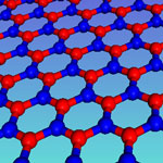 Along with graphene, boron nanoribbons have attracted more and more fundamental research interest. However, a major challenge in providing experimental evidence is that the preparation of atomically thin boron nanoribbons is very difficult. In new work that represents an important step in bridging theoretical predictions and experimental realization of atomically thin boron nanoribbons, reseaerchers demonstrate the successful fabrication of 'white graphene' nanoribbons - made of thermally and chemically stable atomic layers of hexagonal boron nitride - by unwrapping multiwalled boron nanotubes under delicate argon plasma etching. They show that the insulator-semiconductor electrical transition takes place during this processing and that this typically electrically insulating compound becomes a semiconductor when it is in ribbon morphology.
Nov 9th, 2010
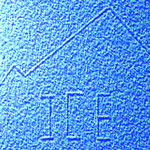 Researchers at Harvard University have shown that nanostructures can be patterned with focused electron or ion beams in thin, stable, conformal films of water ice grown on silicon. They demonstrated ice lithography as a lithographic technique for patterning e.g. metal wires down to 20 nm wide. What's interesting about this technique is that patterning with ices of any condensed gas is a straightforward and practical process. Ice resist does not require spinning or baking. All processing and patterning steps can occur in a single evacuated chamber and be monitored at high resolution. The final removal of unexposed resist leaves minimal residues. Environmentally harmful solvents are not required and complete dry removal of the ice layer can be performed by in situ sublimation. Also, ice lithography makes it possible to nanopattern chemical modifications into silicon and other substrates. The team has now reported the successful application of ice lithography to the fabrication of nanoscale devices.
Nov 4th, 2010
 Many nanotechnology research projects require some form of nanopatterning technique in fabricating the devices, structures and surfaces required. With the current state of micro- and nanofabrication, the direct printing of functional materials is the most efficient method at low cost and low environmental impact. A direct printing approach has the merits of forgoing complex and expensive equipment, reducing the fabrication processes, saving the amount of material used, and removing chemical exposure in the processes. However, imprinting methods suffer from residues and difficulty in multi-alignment. Researchers in Korea have now developed a direct printing technique that is based on a liquid-bridge-mediated transfer moulding process.
Oct 20th, 2010
 Subscribe to our Nanotechnology Spotlight feed