Showing Spotlights 33 - 40 of 65 in category All (newest first):
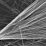
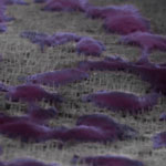 In order to get a true picture of the processes and events that take place inside unmodified, living cells, probing techniques need to be non-destructive, noninvasive and in real-time. Due to their small dimensions, high-aspect ratio nanomaterials such as nanofibers, nanowires and carbon nanotubes are ideal for cellular applications since they can cross the cell membrane without causing significant damage. In particular, semiconductor nanowires attract a lot of interest because of their uniformity, reproducibility and possibility of fine-tuning their intrinsic properties - physical dimensions, crystal structure, electrical and optical properties, etc. Researchers have now shown, for the first time, the spontaneous and close interface of arrays of vertically aligned indium arsenide nanowires with two relevant cell lines, human embryonic kidney cells and rat embryonic dorsal root ganglion neurons.
Mar 14th, 2011
 Nanowires - particularly those of silicon - promise great potentials for high-efficiency, low-cost solar energy conversion. This promise has not yet been met by experimental evidence, raising fundamental questions whether silicon nanowires are intrinsically disadvantaged and whether the photovoltaic research community should continue working on this material. Despite intense efforts, the performance of silicon nanowire-based solar cells remains significantly lower than what has been achieved for bulk silicon or micrometer-scale wires. The gap between the predicted performance and the inability to deliver raises an important question with regard to the origin of this problem. New research shows that the poor performance is not a result of the nanowire morphology, but is intrinsic to the growth chemistry.
Mar 9th, 2011
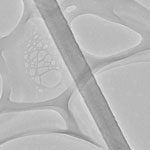
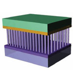
 Nanotechnology-enabled fabrication of solar cells with conventional nanoparticle-based thin-films has a drawback in that the diffusion length of the charge carriers is too short to get charge separation, although the nanoparticles themselves provide copious surface areas; whereas photovoltaic devices fabricated by aligned or partially aligned nanowire array configurations have exhibited enhanced performance owing to improved carrier collection, reduced optical reflection, and efficient absorption. While the nanowire-based approach indeed increases the diffusion length of carriers it also reduces the available surface area. However, being able to fully capture the promising surface and transport properties of nanoscale materials in practical devices or systems relies on the capability of effectively translating the extraordinary characteristics of nanoparticles or nanowires into larger-scale, three-dimensional (3D) structures. Researchers now have come up with a promising approach to address this problem by growing uniformly distributed and high density nanorods into high-aspect ratio nanochannels.
Feb 8th, 2011
 Nanotechnology researchers working on self-powered nanodevices - nanoscale systems that scavenge energy from their surrounding environment - have been experimenting with various power sources ranging from piezoelectric systems to sound. However, the most abundant energy available in biosystems is chemical and biochemical energy, such as glucose. Researchers in China have now reported a nanowire-based biofuel cell based on a single proton conductive polymer nanowire for converting chemical energy from biofluids into electricity, using glucose oxidase and laccase as catalyst. The output of this biofuel cell is sufficient to drive pH, glucose or photon sensors. The high output power, low cost and easy fabrication process, large-scale manufacturability, high 'on-chip' integrability and stability demonstrates its great potential for in vivo biosensing.
Jan 3rd, 2011
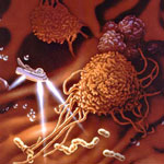 Off-targeting remains a key challenge of researchers working on nanoparticle drug delivery - the majority of intravenously administered therapeutic nanoparticles are also reaching normal tissues, resulting in considerable adverse side effects. Another challenge of nanoparticle drug delivery includes the limited penetration depth of particles into the tumors. While extensive efforts have been devoted for designing therapeutic nanoparticles, a new study - echoing the journey through the human body in Fantastic Voyage - represents the first example of coupling such drug nanocarriers with self-propelled nanoshuttles. The ability of synthetic nanomotors to carry 'cargo' has already been demonstrated; but not in connection to common drug-loaded particles. In a new study, researchers demonstrate that catalytic nanoshuttles can readily pickup common biocompatible and biodegradable drug-loaded particles and liposomes and transport them over predefined routes towards predetermined destination.
Dec 10th, 2010
 Zinc oxide is considered a workhorse of technological development exhibiting excellent electrical, optical, and chemical properties with a broad range of applications as semiconductors, in optical devices, piezoelectric devices, surface acoustic wave devices, sensors, transparent electrodes, solar cells, antibacterial activity etc. Thin films or nanoscale coating of ZnO nanoparticles are viewed with great interest for their many potential applications as substrates for functional coatings. Researchers in Taiwan have now shown, for the first time, that they can directly grow vertically aligned, highly crystalline and defect-free single-crystalline zinc oxide nanorods and nanoneedles on paper.
Oct 6th, 2010
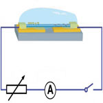
 Traditionally, battery materials have been studied with bulk quantities in a complex environment with both active electrode components and many other supporting materials such as polymer binders and conductive additives. Although nanomaterials have been found to be able to improve battery performance, the complexity has made it hard to tell clearly about their advantages. Moreover, it is difficult to know whether fast capacity fading is due to the intrinsic nature of the transport property changes of active nanomaterials or an extrinsic reason from their interactions with the supporting materials, if all of them are studied together. The goal to understand the intrinsic reason of active material capacity fading has motivated a group of researchers to design single nanowire electrochemical devices as an extremely simplified model system to push the fundamental limits of the nanowire materials for energy storage applications. The result is a powerful and effective diagnostic tool for property degradation of lithium ion based energy storage devices.
Sep 27th, 2010
 Imagine cellular phones that can be charged during conversations and sound-insulating walls near highways that generate electricity from the sound of passing vehicles. A number of approaches for self-powering systems by scavenging energy from environments using photovoltaic, thermoelectric, and piezoelectric phenomena have been intensively explored. Among them, very recent innovative research has been intensively carried out to convert external mechanical stimuli such as body movements, heartbeat, blood flow, and ultrasonic wave into electricity, resulting in piezoelectric power-driven wireless self-powered systems. Such a piezoelectric power generation aims to capture the normally wasted energy surrounding a system and converts it into usable energy for operating electrical devices. New work by a nanotechnology research team in Korea has now demonstrated that it is possible to use sound as a power source to drive nanogenerators based on piezoelectric nanowires.
Sep 23rd, 2010
 Subscribe to our Nanotechnology Spotlight feed