Bismuthene: The Heavy-Element 2D Material Redefining Topological Electronics
What is Bismuthene?
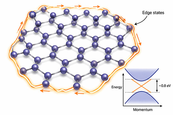
Bismuthene is a two-dimensional (2D) material consisting of a single layer or few layers of bismuth atoms arranged in a honeycomb lattice, analogous to the structure of graphene. As the heaviest stable element used to fabricate 2D nanomaterials, bismuth brings exceptionally strong spin-orbit coupling (SOC) to the 2D materials family.
This strong SOC gives bismuthene a topological energy gap of approximately 0.8 electron volts – large enough to sustain quantum spin Hall behavior at room temperature. That gap is far larger than those of related Xenes such as stanene and antimonene, making bismuthene one of the most actively studied elemental 2D materials.
Crystal Structure and Allotropes
Bulk bismuth has a rhombohedral crystal structure with puckered layers held together by van der Waals forces. When thinned to a monolayer, bismuth can adopt two principal structural phases. The α-phase (also called the buckled honeycomb or Bi(111) structure) resembles a corrugated version of graphene, with two sublattice atoms offset vertically. The β-phase (sometimes referred to as the black-phosphorus-like or Bi(110) structure) features a rectangular puckered lattice with stronger in-plane anisotropy.
Both allotropes are dynamically stable, as confirmed by density functional theory (DFT) phonon dispersion calculations showing no imaginary modes. Molecular dynamics simulations indicate that free-standing bismuthene remains structurally intact at temperatures well above 300 K, with thermal instability setting in only around 700 K. The choice of substrate can favor one phase over another: epitaxial growth on SiC(0001), for example, produces the honeycomb α-phase, while growth on certain metallic substrates can stabilize the β-phase.
How Spin-Orbit Coupling Shapes Bismuthene
The defining physical feature of bismuthene is the strong SOC that arises from the high atomic number (Z = 83) of bismuth. In lighter 2D materials such as silicene or germanene, SOC opens only tiny bandgaps (on the order of millielectron volts), requiring cryogenic temperatures to observe topological effects. In bismuthene grown on SiC, a synergy between the flat honeycomb geometry, strong SOC, and an orbital filtering effect mediated by the substrate produces a bulk gap of approximately 800 meV – the largest experimentally determined topological gap reported for any 2D material.
This gap inversion transforms bismuthene into a topological insulator: the interior of the sheet is electrically insulating, while the edges host helical conducting states whose spin orientation is locked to the direction of electron momentum. Because the gap is so large, these edge states survive thermal fluctuations at room temperature, distinguishing bismuthene from virtually all other known quantum spin Hall systems.
Synthesis Methods
Bismuthene can be produced through both top-down and bottom-up approaches, each offering different trade-offs between crystal quality, scalability, and cost.
Mechanical and Liquid-Phase Exfoliation
Mechanical exfoliation of bulk bismuth crystals can yield few-layer bismuthene flakes suitable for fundamental studies. Liquid-phase exfoliation, often assisted by sonication in appropriate solvents such as N-methyl-2-pyrrolidone or isopropanol, produces nanosheets in larger quantities. Ice-bath sonication has proven effective for generating ultrathin bismuthene suitable for electrochemical applications, though controlling layer number and lateral dimensions remains challenging.
Epitaxial Growth
Molecular beam epitaxy (MBE) on SiC(0001) substrates produces the highest-quality monolayer bismuthene with the honeycomb structure needed to realize the large topological gap. Chemical vapor deposition (CVD) and pulsed laser deposition (PLD) offer additional routes for growing large-area films, although controllability, growth rates, and cost remain active areas of optimization.
Wet-Chemical Synthesis
Solution-based methods, including solvothermal reduction of bismuth salts, can yield bismuthene nanosheets with tunable thickness and surface chemistry. These approaches are attractive for applications in catalysis and energy storage, where large volumes of material are needed and single-crystal perfection is less critical than in electronic devices.
Significance in Nanotechnology
Bismuthene occupies a unique position in the landscape of 2D materials. Its combination of topological electronic states, strong SOC, low toxicity compared to other pnictogen Xenes such as arsenene, and good air stability relative to phosphorene makes it a compelling platform for both fundamental physics and applied nanotechnology. The high surface-to-volume ratio inherent to its 2D geometry amplifies surface-driven phenomena such as catalytic activity and molecular adsorption, while quantum confinement in the out-of-plane direction gives rise to layer-dependent optical bandgaps spanning roughly 0.18 to 2.6 eV.
Key Properties
Electronic and Topological Properties
Monolayer bismuthene is a 2D topological insulator with helical edge states protected by time-reversal symmetry. The theoretical electronic bandgap of free-standing bismuthene is about 0.99 eV, suitable for semiconductor applications. On SiC substrates, the substrate-mediated orbital filtering widens the topological gap to ~800 meV. Bulk bismuth itself has been identified as a higher-order topological insulator, hosting one-dimensional conducting hinge states protected by rotational and inversion symmetries.
Optical Properties
Bismuthene exhibits layer-dependent direct bandgaps, enabling tunable light absorption across a broad spectral range from the visible to the infrared. The material shows strong third-order nonlinear optical responses, including saturable absorption behavior that extends into the near-infrared region. These nonlinear optical properties make bismuthene attractive for ultrafast laser applications, where it can function as a saturable absorber for mode-locking in pulsed laser systems.
Carrier Mobility and Transport
Few-layer bismuthene possesses high charge carrier mobility, which, combined with the topological protection of its edge channels, supports low-dissipation electron transport. The ballistic nature of the helical edge states means that electrons traveling in opposite directions carry opposite spin orientations, suppressing backscattering in the absence of magnetic perturbations. This spin-momentum locking is central to proposed spintronic device concepts.
Stability
Compared to phosphorene, which degrades rapidly in ambient conditions, bismuthene exhibits superior air stability. Few-layer bismuthene retains its structural integrity and electronic properties under ambient exposure for extended periods. For epitaxial monolayer bismuthene on SiC, encapsulation with a protective graphene overlayer has been demonstrated to preserve both the structural and topological properties while shielding the material from oxidation.
Applications
Spintronics and Topological Electronics
The room-temperature quantum spin Hall effect in bismuthene opens a pathway to dissipationless spin transport in nanoelectronic circuits. Helical edge channels could serve as interconnects that carry spin-polarized currents without the resistive losses of conventional conductors. Bismuthene nanoribbons have been studied theoretically and experimentally as building blocks for topological transistors and quantum interference devices.
Electrocatalysis and Photocatalysis
The enlarged surface area and favorable electrochemical activity of 2D bismuthene make it an efficient catalyst for CO2 reduction to formate and other value-added chemicals, as well as for nitrogen fixation. In photocatalytic applications, bismuthene-based heterostructures enhance charge separation and electron transfer efficiency, improving selectivity toward products such as methane and formic acid. The material has also shown strong performance in photocatalytic degradation of organic pollutants under visible light.
Energy Storage
Few-layer bismuthene produced by liquid exfoliation has demonstrated promising cyclability as an anode material for sodium-ion batteries, where the intercalation and alloying processes benefit from the 2D geometry. Bismuthene nanosheets also serve as electrode materials for supercapacitors, exploiting the high surface area and good electrical conductivity of the ultrathin sheets.
Biomedical Applications
Bismuth-based compounds have a long clinical history, and bismuthene inherits this low toxicity profile, distinguishing it from arsenene and other pnictogen Xenes. The strong near-infrared absorption and high photothermal conversion efficiency of bismuthene nanosheets make them candidates for photothermal and photodynamic cancer therapy. Bismuthene has also been explored as a carrier for nanomedicine drug delivery, where its large surface area enables high drug loading capacity and its biodegradability supports safe clearance from the body.
Photonics and Sensing
The broadband nonlinear optical response of bismuthene has been exploited in mode-locked fiber lasers, producing ultrashort pulses with pulse widths shorter than those achieved with many other 2D saturable absorbers. Bismuthene-based photodetectors have shown sensitivity across visible and infrared wavelengths. In sensing, bismuthene nanosheets serve as transduction elements in electrochemical sensors for detecting heavy metals, biomolecules, and gases.
Challenges and Future Perspectives
Despite its attractive properties, bismuthene faces several challenges on the path to practical devices. Scalable synthesis of large-area, high-quality monolayer bismuthene with controlled crystal phase remains difficult. While MBE on SiC yields excellent topological properties, the process is expensive and not easily integrated into industrial fabrication workflows. CVD and PLD approaches need further optimization to achieve the uniformity and crystalline quality required for electronic applications.
Environmental stability, though better than phosphorene, is still a concern for monolayer bismuthene in ambient air over long timescales. Encapsulation strategies, such as graphene capping or integration into van der Waals heterostructures with hexagonal boron nitride, are being explored to extend device lifetimes. Characterization of bismuthene also benefits from advanced techniques including scanning tunneling microscopy, angle-resolved photoemission spectroscopy, and Raman spectroscopy, which together provide detailed information on band structure, phonon dynamics, and topological edge states.
Future research will focus on integrating bismuthene with other 2D materials to form moiré superlattices and functional heterostructures, where interlayer coupling can be used to tune topological, electronic, and catalytic properties on demand. The development of heteroatom-doped bismuthene variants – incorporating nitrogen, sulfur, or other elements – is an active direction for enhancing electrocatalytic performance. As synthesis methods mature and device architectures evolve, bismuthene is positioned to become a key material in the broader toolkit of quantum technologies, sustainable energy conversion, and advanced electronics.
Further Reading
Science, Bismuthene on a SiC substrate: A candidate for a high-temperature quantum spin Hall material
Chemical Society Reviews, Advances of 2D bismuth in energy sciences
Journal of Materials Chemistry C, Recent advances in ecofriendly 2D monoelemental bismuthene as an emerging material for energy, catalysis and biomedical applications
