Nanofilms: Ultra-Thin Layers Revolutionizing Electronics, Optics, and Beyond
What are Nanofilms?
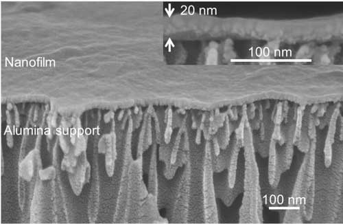
Nanofilms are ultra-thin layers of material with thicknesses ranging from a few nanometers to several hundred nanometers. These films exhibit unique properties and behaviors that differ from their bulk counterparts due to their reduced dimensionality and high surface-to-volume ratio. Nanofilms can be composed of various materials, including metals, semiconductors, polymers, and ceramics, and are fabricated using advanced deposition techniques such as physical vapor deposition (PVD), chemical vapor deposition (CVD), and atomic layer deposition (ALD).
Key Features of Nanofilms
Nanofilms possess several key features that distinguish them from bulk materials:
- Thickness: The nanoscale thickness of these films, typically ranging from 1-100 nm, is a defining characteristic that leads to their unique properties.
- High Surface Area: The high surface-to-volume ratio of nanofilms results in a significant portion of the atoms being located at the surface, making them highly sensitive to their environment and enabling enhanced surface interactions.
- Quantum Confinement: When the thickness of a nanofilm approaches the nanoscale, quantum confinement effects can emerge, leading to changes in the electronic, optical, and magnetic properties of the material.
- Interfacial Effects: The interfaces between nanofilms and their substrates or between multiple nanofilm layers play a crucial role in determining their overall properties and performance.
Fabrication Methods
Nanofilms can be fabricated using various deposition techniques, each with its own advantages and limitations:
Physical Vapor Deposition (PVD)
PVD techniques, such as sputtering and thermal evaporation, involve the physical vaporization of a target material and its subsequent condensation onto a substrate to form a thin film. PVD methods offer high purity, good adhesion, and the ability to deposit a wide range of materials.
Chemical Vapor Deposition (CVD)
CVD involves the chemical reaction of gaseous precursors on a heated substrate to form a thin film. CVD techniques, such as plasma-enhanced CVD (PECVD) and low-pressure CVD (LPCVD), enable the deposition of high-quality, conformal films with excellent step coverage.
Atomic Layer Deposition (ALD)
ALD is a highly precise and controlled deposition method that involves the sequential introduction of gaseous precursors to a substrate, resulting in the layer-by-layer growth of ultra-thin films. ALD offers exceptional thickness control, conformality, and the ability to deposit films with thicknesses down to a few angstroms.
Properties and Applications
Nanofilms exhibit a wide range of unique properties that make them valuable for various applications:
Electronic Properties
Nanofilms can display enhanced electronic properties, such as high electron mobility, low resistivity, and tunable bandgaps. These properties make them suitable for applications in thin-film transistors, transparent conductors, and flexible electronics.
Optical Properties
The optical properties of nanofilms, such as refractive index, absorption, and transmission, can be tailored by controlling their thickness and composition. This makes them valuable for applications in optical coatings, anti-reflective surfaces, and plasmonic devices.
Mechanical Properties
Nanofilms can exhibit enhanced mechanical properties, such as high hardness, wear resistance, and low friction. These properties are exploited in protective coatings, tribological applications, and micro-electromechanical systems (MEMS).
Catalytic Properties
The high surface area and nanoscale features of nanofilms make them attractive for catalytic applications. Nanofilms of noble metals, metal oxides, and other materials are used in heterogeneous catalysis, fuel cells, and environmental remediation.
Challenges and Future Perspectives
Despite the significant progress in nanofilm technology, several challenges remain to be addressed. One of the main challenges is the scalability and reproducibility of nanofilm fabrication processes. Ensuring uniform thickness, composition, and properties over large areas is crucial for the successful integration of nanofilms into practical devices.
Future research in nanofilms will focus on the development of novel materials and deposition techniques to enable the fabrication of high-quality, multifunctional nanofilms. The integration of nanofilms with other nanomaterials, such as nanoparticles and nanowires, will lead to the development of advanced nanocomposite films with enhanced properties. Additionally, the exploration of nanofilm-based devices for emerging applications, such as flexible electronics, wearable sensors, and energy harvesting, will drive the continued growth and impact of nanofilm technology.
Further Reading
International Applied Mechanics, Nanofilms: Structural Features and Nanoindentation Methods
Nanomaterials, The Applications of Ultra-Thin Nanofilm for Aerospace Advanced Manufacturing Technology
Key Engineering Materials, Preparation and Characterization of Nano-Films Materials
