| Jun 01, 2023 |
Functional 2D-enabled microchips become reality(Nanowerk News) The first demonstration of a functional microchip integrating atomically thin two-dimensional materials with exotic properties heralds a new era of microelectronics. |
| The world’s first fully integrated and functional microchip based on exotic two-dimensional materials has been fabricated at KAUST. The breakthrough demonstrates the potential of 2D materials to expand the functionality and performance of microchip-based technologies. |
| Since the first fabrication of atomically thin layers of graphite — called graphene — in 2004, there has been intense interest in such materials for advanced and novel applications due to their exotic and promising physical properties. But, despite two decades of research, functional microdevices based on these 2D materials have proved elusive due to the challenges in fabricating and handling such fragile thin films. |
| Inspired by recent achievements in the Lanza’s lab on functional 2D films, the collaboration has now produced and demonstrated a prototype 2D-based microchip. |
| The findings have been published in Nature ("2D–CMOS microchips for memristive applications"). |
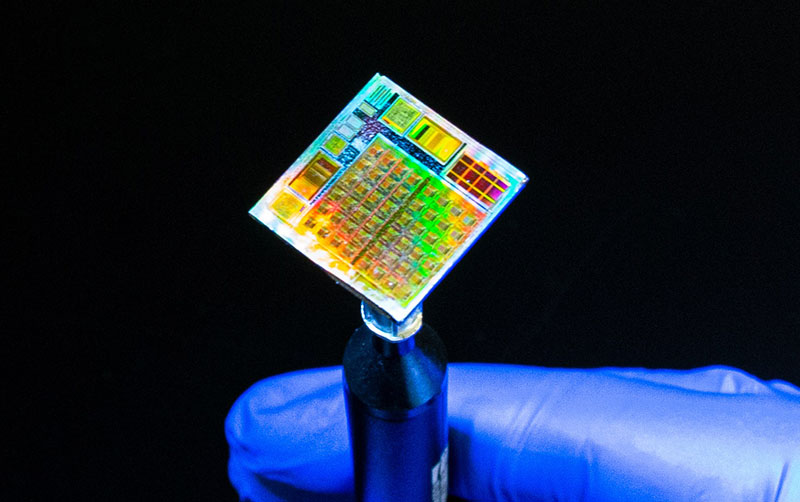 |
| The world's first 2D microchip using synthetic materials. (Image: Mario Lanza) |
| “Our motivation was to increase the technology readiness level of 2D material-based electronic devices and circuits by using conventional silicon-based CMOS microcircuits as a base and standard semiconductor fabrication techniques,” says Lanza. “The challenge, however, is that synthetic 2D materials can contain local defects such as atomic impurities that can cause small devices to fail. Also, it is very difficult to integrate the 2D material into the microchip without damaging it.” |
| The research team optimized the design of the chip to make it easier to fabricate and minimize the effect of defects. They did this by fabricating standard complementary metal oxide semiconductor (CMOS) transistors on one side of the chip and feeding interconnects through to the underside, where the 2D material could be transferred reliably in small pads less than 0.25 micrometers across. |
| “We produced the 2D material — hexagonal boron nitride, or h-BN, on copper foil — and transferred it to the microchip using a low-temperature wet process, and we then formed electrodes over the top by conventional vacuum evaporation and photolithograpy, which are processes we have in-house,” says Lanza. “In this way we produced a 5×5 array of one-transistor/one-memristor cells connected in a crossbar matrix.” |
| The exotic properties of 2D h-BN, here just 18 atoms or 6 nanometers thick, make it an ideal memristor — a resistive component whose resistance can be set by the applied voltage. In this 5×5 arrangement, each of the microscale memristor pads is connected to a single dedicated transistor. This provides the fine voltage control needed to operate the memristor as a functional device with high performance and reliability over thousands of cycles, in this case as a low-power neural network element. |
| Source: KAUST (Note: Content may be edited for style and length) |

