| Posted: Feb 05, 2010 |
Graphene-inspired bismuth telluride atomic layers could revolutionize cooling and topological insulator applications |
| (Nanowerk Spotlight) Bismuth telluride and its alloys are unique materials. They are the best thermoelectric materials known today, and they are as important to the thermoelectric industry – for cooling and energy generation applications – as silicon is important to the electronic industry. It has been predicted theoretically that structuring bismuth telluride into crystalline ultra-thin films (with the thickness of few nanometers) would lead to a drastic improvement of the thermoelectric figure of merit (denoted as ZT), which defines the efficiency of the thermoelectric energy conversion. The improvement comes as a result of the strong quantum confinement of charge carriers and reduction of the thermal conductivity. In addition to their thermoelectric applications, bismuth telluride thin films recently attracted attention as promising topological insulators – a newly discovered class of materials with unusual properties. |
| Electrical engineering professor Alexander Balandin and researchers from his Nano-Device Laboratory at the University of California - Riverside (UCR), became the first who succeeded in 'graphene-inspired' mechanical exfoliation of atomically-thin crystals of bismuth telluride, also referred to as quasi-two-dimensional (2D) crystals. |
| Balandin, who also serves as a Chair of Materials Science and Engineering at UCR, explains the importance of such exfoliation to Nanowerk: "Conventional growth techniques for bismuth telluride cannot provide the films with the properties, e.g. crystallinity, thickness of ∼1 nm and high potential barriers, required for strong confinement of charge carriers and thermal conductivity reduction. Without such confinement you cannot achieve the theoretically predicted improvement in the thermoelectric properties." |
| The preliminary results of this work were published in the February 1, 2010 online issue of Applied Physics Letters and featured on the cover of its February 2010 issue ("Atomically-thin crystalline films and ribbons of bismuth telluride"). |
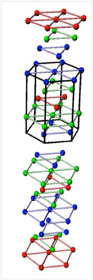 |
| Figure 1: Crystal structure of bismuth telluride showing a single quintuple separated from other layers by van der Waals gaps. (Image: Balandin group, UCR) |
| In this work, the UCR research team performed 'graphene-like' mechanical exfoliation of crystalline bismuth telluride films with a thickness of a few atoms. The atomically thin films were suspended across trenches in silison/silicon oxide substrates, and subjected to detail material characterization. The presence of van der Waals gaps, i.e. spots with weak binding between some atomic planes (see Figure 1) allowed them to disassemble a bismuth telluride crystal into its quintuple building blocks – five mono-atomic sheets – consisting of Te-Bi-Te-Bi-Te atomic planes. By altering the thickness and sequence of atomic planes, Balandin's group was able to create 'designer' non-stoichiometric quasi-2D crystalline films, change their composition and doping, the type of charge carriers as well as other properties. |
| Balandin used to conduct theoretical thermoelectric research years ago. Because of this, he knew that if he can achieve the fabrication of crystalline bismuth telluride films with the thickness down to about 1 nm there would be a good possibility that a major improvement in the thermoelectric figure of merit could be achieved. |
| "For the past there years, my group was mostly involved in graphene research" says Balandin (see our Spotlights on some of his previous work: "Graphene transistors can work without much noise" or "Just looking at graphene can change its properties"). "We have prepared our graphene samples by the mechanical exfoliation technique, i.e. cleavage from bulk graphite, which is now a standard procedure to obtained high-quality graphene. One day, about two years ago, I thought: what if I apply the same approach to other materials. I remembered that bismuth telluride should have layers weakly bound by van der Waals forces. I shared this idea with a PhD student under my supervision, Desalegne Teweldebrhan. That was enough to motivate him to put some extra hours into research working on bismuth telluride simultaneously with his work on graphene." |
| During a several-month period, Desalegne managed to produce atomically thin films of bismuth telluride. Their crystalline and electrical properties were verified with the help of other PhD students in Balandin's lab – Vivek Goyal and Muhammad Rahman. The group delayed publishing their results while preparing a patent application and collecting more data. |
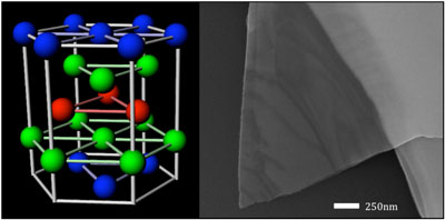 |
| Figure 2: Schematic of a single atomic quintuple (left) of bismuth telluride and scanning electron microscopy image of the atomically thin film made of this material by mechanical exfoliation. (Image: Balandin group, UCR) |
| Balandin points out that one of the problems associated with the process of producing such atomically-thin films is accurate counting of the number of atomic planes, i.e. layers, in the obtained films. The physical properties of such films depend strongly on the number of atomic layers, which explains the importance of this knowledge. |
| "The number of atomic layers in graphene, for example, can be accurately determined with Raman spectroscopy," says Balandin. "We tried to use a similar technique with the bismuth telluride films, but encountered all sorts of problems because the new material is not as robust as graphene and has entirely different Raman signatures. Eventually though we were able to find the Raman spectral features which can be used as indicators of atomically-thin films. These results will appear in print soon." |
| The approach for bismuth telluride quasi-2D crystal identification proposed by Balandin could become a new standard for bismuth telluride nanometrology. |
| The atomically-thin films fabricated by Balandin's group could find applications in thermoelectric devices and help to increase the thermoelectric figure of merit (ZT). The best commercial thermoelectric materials today have a figure of merit of about 1 at room temperature. Balandin says that it was theoretically predicted that if ZT increases to about 3, the thermoelectric power generation and cooling will become competitive with conventional colling technology. |
| "If ZT is enhanced that much, there will be a revolution: imagine that we all will have to throw away our refrigerators and buy new thermoelectric ones, which do not have moving parts and can work really long time" says Balandin. |
| Atomically thin thermoelectric bismuth telluride films could also be used for on-spot cooling of electronic chips (see Balandin?s review of the thermal management problems in electronics in the feature published by IEEE Spectrum: "Better Computing Through CPU Cooling"). |
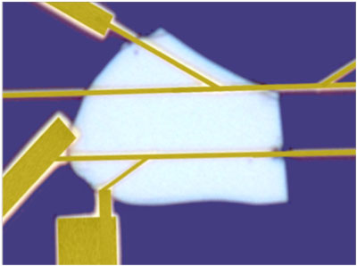 |
| Figure 3: Crystalline bismuth telluride film with metal contacts fabricated for measurements of electrical properties. (Image: Balandin group, UCR) |
| Most recently, the interest for the stacked quasi-2D layers of bismuth telluride received an additional boost from an unexpected direction. It has been shown that bismuth telluride is a member of a new type of recently discovered materials referred to as topological insulators. The surface state of a quasi-2D crystal of bismuth telluride is predicted to consist of a single Dirac cone. Moreover, it has been shown that the layered structures of related materials such as bismuth telluride and antimony telluride are also topological insulators. The particles in topological insulators coated with thin ferromagnetic layers have manifested exotic physics and were proposed for possible applications in electronics. |
| "The news about topological insulators makes our work on mechanical exfoliation of bismuth telluride quintuples even more interesting," says Balandin. "My students are now enthusiastically examining both possible applications – thermoelectric and topological insulators." |
| He notes that his team has already had some preliminary results demonstrating enhancement of the thermoelectric figure of merit in their films at room temperature and below. "We plan to verify it in a number of samples and build a prototype cooler capable of operating in a wide temperature range." |
 By
Michael
Berger
– Michael is author of four books by the Royal Society of Chemistry:
Nano-Society: Pushing the Boundaries of Technology (2009),
Nanotechnology: The Future is Tiny (2016),
Nanoengineering: The Skills and Tools Making Technology Invisible (2019), and
Waste not! How Nanotechnologies Can Increase Efficiencies Throughout Society (2025)
Copyright ©
Nanowerk LLC
By
Michael
Berger
– Michael is author of four books by the Royal Society of Chemistry:
Nano-Society: Pushing the Boundaries of Technology (2009),
Nanotechnology: The Future is Tiny (2016),
Nanoengineering: The Skills and Tools Making Technology Invisible (2019), and
Waste not! How Nanotechnologies Can Increase Efficiencies Throughout Society (2025)
Copyright ©
Nanowerk LLC
|

Become a Spotlight guest author! Join our large and growing group of guest contributors. Have you just published a scientific paper or have other exciting developments to share with the nanotechnology community? Here is how to publish on nanowerk.com. |
