| Posted: Jan 29, 2013 |
Printable photonic devices with resolution below 10 nanometers |
| (Nanowerk Spotlight) With the current state of micro- and nanofabrication, the direct printing of functional materials is the most efficient method at low cost and low environmental impact. A direct printing approach has the merits of forgoing complex and expensive equipment, reducing the fabrication processes, saving the amount of material used, and removing chemical exposure in the processes. |
| A key benefit of nanoimprint lithography is its sheer simplicity. There is no need for complex optics or high-energy radiation sources with a nanoimprint tool. There is no need for finely tailored photoresists designed for both resolution and sensitivity at a given wavelength. The simplified requirements of the technology allow low-cost, high-throughput production processes of various nanostructures with operational ease. |
| NIL already has been applied in various fields such as biological nanodevices, nanophotonic devices, organic electronics, and the patterning of magnetic materials. Especially the nanopatterning of high refractive index optical films promises the development of novel photonic nanodevices such as planar waveguide circuits, nano-lasers, solar cells and antireflective coatings. |
| A team of researchers and engineers have now developed a robust route for high-throughput, high-performance nanophotonics based direct imprint of high refractive index, low visible wavelength absorption materials. |
| "The core of our development is a process for patterning films with high refractive and high optical transparency which is suitable for fabricating printable photonic devices," Christophe Peroz, Director of Nanofabrication and Optical Devices at aBeam Technologies, tells Nanowerk. "We have developed an imprint material specifically optimized for creating crack-free films which are imprintable at high resolution and with high optical performances. Especially the very high values of refractive index are important to creating novel nanophotonic structures like photonic crystal in visible light." |
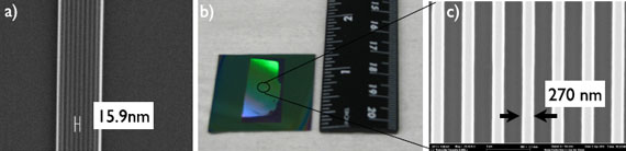 |
| Example of nanostructures imprinted onto TiO2 films: (a) scanning electron microscope (SEM) image of a grating with 8 nm line width and 16 nm pitch before post-imprint annealing; (b) optical micrograph of a 700 nm pitch grating imprinted onto TiO2 films over 1 in2 and (c) a SEM picture of the grating. (Reprinted with permission from IOP Publishing) |
| This work, reported in the January 22, 2013 online edition of Nanotechnology ("A route for fabricating printable photonic devices with sub-10 nm resolution"), demonstrates that direct imprint of functional films is a potential route for developing low-cost printable photonic nanodevices. |
| This work was led by The Molecular Foundry, in collaboration with aBeam Technologies in the framework of a Small Business Technology Transfer project funded by US Air Force Office of Scientific Research |
| The team developed a titanium-based inorganic-organic hybrid material for imprinting TiO2 crack-free films over a large area. Their novel process allows the patterning of TiO2 films with feature sizes down to 5 nm. |
| "We show the optical properties of the imprinted photonic films can easily be tuned with a simple post-annealing step and are suitable for fabricating printable photonic devices," Peroz notes. "The optical properties are outstanding and the resolution achieved is the highest reported in the literature and defines the state-of-the-art." |
| The team's novel strategy to pattern optical functional films with high refractive index over large areas is reported starts by synthesizing a special hybrid TiO2-based resin. Then, films are spin-coated and soft baked in order to create uniform solvent-free films – the film thickness can be varied from 20 nm up to 1 µm depending on the concentration of the titania precursor. These films can be imprinted at low pressure and cured under UV light. By using different time intervals and annealing temperatures, the optical properties – i.e. refractive index and extinction coefficient – of the films can be adjusted. |
| "The optical properties of the nanostructured films are easily tuned by post annealing and their optical transparency is suitable with photonic applications," Peroz summarizes the results. "This opens a promising route for fabricating printable photonic nanodevices with high resolution and high throughput." |
| Potential applications of this material are printable integrated devices – waveguide, resonator, planar holograms; antireflective coating with applications in solar cells; and light extraction for LEDs. |
 By
Michael
Berger
– Michael is author of four books by the Royal Society of Chemistry:
Nano-Society: Pushing the Boundaries of Technology (2009),
Nanotechnology: The Future is Tiny (2016),
Nanoengineering: The Skills and Tools Making Technology Invisible (2019), and
Waste not! How Nanotechnologies Can Increase Efficiencies Throughout Society (2025)
Copyright ©
Nanowerk LLC
By
Michael
Berger
– Michael is author of four books by the Royal Society of Chemistry:
Nano-Society: Pushing the Boundaries of Technology (2009),
Nanotechnology: The Future is Tiny (2016),
Nanoengineering: The Skills and Tools Making Technology Invisible (2019), and
Waste not! How Nanotechnologies Can Increase Efficiencies Throughout Society (2025)
Copyright ©
Nanowerk LLC
|

Become a Spotlight guest author! Join our large and growing group of guest contributors. Have you just published a scientific paper or have other exciting developments to share with the nanotechnology community? Here is how to publish on nanowerk.com. |
