| Posted: Jan 02, 2008 |
New photonic nanostructures enable blue-violet surface-emitting lasers |
| (Nanowerk Spotlight) Semiconductors can be used as small, highly efficient photon sources such as laser diodes and light-emitting diodes (LEDs). Such semiconductor photon sources find application in displays, optical storage, communications, printing, surveying, and as small efficient optical pumps for other optical processes. These lasers operate in the near infrared wavelength of 700-1400 nanometers and in the upper bands (red and green) of the visible spectrum. |
| Semiconductor lasers can be grouped into two classes: Edge-emitting lasers, where the laser light is propagating parallel to the wafer surface of the semiconductor chip and is reflected or coupled out at a cleaved edge; and surface-emitting lasers, where the light propagates in the direction perpendicular to the semiconductor wafer surface. Surface-emitting lasers are the newer type of semiconductor lasers. In order to push optical electronics to the next level of development, many scientists pin their hopes on photonic crystals as a highly anticipated future optical technology. |
| Photonic crystals are periodic optical (nano)structures that are designed to affect the motion of photons in a similar way that periodicity of a semiconductor crystal affects the motion of electrons. Photonic crystal allow the fabrication of photonic-crystal surface-emitting lasers (PC-SELs). These PC-SELs have several outstanding features: first, perfect, single longitudinal, and lateral mode oscillation can be achieved even when the lasing area becomes very large; and second, the polarization mode and the beam pattern can be controlled by appropriate design of the unit cell and/or lattice phase in the two-dimensional (2D) photonic crystal. While shorter-wavelength surface-emitting laser sources are important for a variety of fields including photonics, information processing and biology, the shortest lasing wavelength achieved so far with PC-SELs is 980 nm (near-infrared). |
| Researchers in Japan now report on the realization of a current-driven blue-violet photonic crystal surface-emitting laser, opening the door to a much wider range of applications for this type of lasers. |
| Photonic crystals – also known as photonic band gap material – are similar to semiconductors, only that the electrons are replaced by photons (i.e. light). By creating periodic structures out of materials with contrast in their dielectric constants, it becomes possible to guide the flow of light through the photonic crystals in a way similar to how electrons are directed through doped regions of semiconductors. The photonic band gap (that forbids propagation of a certain frequency range of light) gives rise to distinct optical phenomena and enables one to control light with amazing facility and produce effects that are impossible with conventional optics. |
| In addition to this band gap, photonic band edge – at which a photonic band gap starts to appear &nd also provides an important feature to control photons, where the group velocity of light becomes zero and a two-dimensional large-area cavity mode can be constructed. |
| Along the way to all-optical devices in communication and information technology, photonic crystals play a significant role. They form a basis material for the future realization of optical components and circuits, and maybe even complex optical circuits or optical computers. |
| "Shorter-wavelength surface-emitting laser sources are important for a variety of fields including photonics, information processing and biology." Dr. Susumu Noda explains to Nanowerk. "We were successful in developing a current-driven blue-violet photonic crystal surface-emitting laser. We have developed a fabrication method, named 'air holes retained over growth' (AROG), in order to construct a two-dimensional gallium nitride/air photonic crystal structure. The resulting periodic structure has a photonic crystal band-edge effect sufficient for the successful operation of a current-injection surface-emitting laser." |
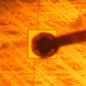 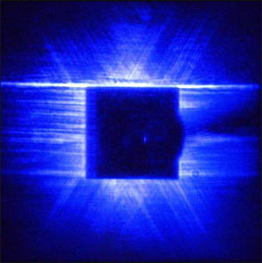 |
| Left: Image of device surface, where current was not injected, (before lasing oscillation). Central square (100µmx100µm) is electrode. Right: Near-field pattern after lasing oscillation. Large area blue-violet lasing oscillation has been successfully achieved. (Images: Dr. Noda) |
| This represents an important step in the development of laser sources – from both a scientific and engineering point of view – that could be focused to a size much less than the wavelength and be integrated two-dimensionally at such short wavelengths. Noda points out that this is the first report of the successful operation of a current-driven gallium nitride (GaN)-based blue-violet SEL. |
| Noda is a Professor in the Department of Electronic Science and Engineering and the Vice Director of the Photonics and Electronics Science and Engineering Center at Kyoto University in Japan. His latest research findings titled "GaN Photonic-Crystal Surface-Emitting Laser at Blue-Violet Wavelengths" have been published in the December 20, 2007 online edition of Science. |
| "One issue in the realization of a gallium nitride (GaN)-based PC-SEL has been whether a 2D photonic crystal structure could be constructed with a sufficient band-edge effect" says Noda. "To do so requires the fabrication of a high-quality 2D GaN/air periodic structure with a lattice constant of between 100 and 200 nm, close to an active layer with optical gain. In order to obtain the required band-edge effect, the PC structure must be constructed within 300 nm of the active layer." |
| Noda explains that, previously, 2D semiconductor/air photonic crystal structures in PC-SELs have generally been constructed using a wafer-fusion technique where one of the important processes is to remove the sacrificial substrate after the 2D semiconductor/air periodic structure has been formed. |
| "Although there are several reports on sacrificial etching techniques in GaN systems, applying these processes for the fabrication of PC-SELs has not yet been established" he notes. "We therefore developed our new AROG method for the construction of such a periodic structure. Our method is based on the particular characteristics of GaN growth, namely that the growth proceeds much faster in the lateral direction than it does vertically from the (0001) crystal plane." |
| At present, the laser operates with a large threshold current, however, the performance could be improved significantly by three methods that Noda and his group have described: 1) Improvement of the crystalline quality of the multiple-quantum-well active layer. 2) Optimization of the distance between the active layer and photonic crystal. Currently, the distance is ∼150 nm, and the degree of mode overlap with the air holes is limited to be ∼3.5% . If this distance was reduced to, for example, ∼60 nm, the band edge effect could be increased, causing the threshold current to be reduced significantly. 3) Employment of a transparent electrode. Currently, the top electrode is not transparent and thus blocks much of the surface emission. When the transparent electrode (or ring-type electrode) is employed, the output power and/or efficiency could be improved. |
 By
Michael
Berger
– Michael is author of four books by the Royal Society of Chemistry:
Nano-Society: Pushing the Boundaries of Technology (2009),
Nanotechnology: The Future is Tiny (2016),
Nanoengineering: The Skills and Tools Making Technology Invisible (2019), and
Waste not! How Nanotechnologies Can Increase Efficiencies Throughout Society (2025)
Copyright ©
Nanowerk LLC
By
Michael
Berger
– Michael is author of four books by the Royal Society of Chemistry:
Nano-Society: Pushing the Boundaries of Technology (2009),
Nanotechnology: The Future is Tiny (2016),
Nanoengineering: The Skills and Tools Making Technology Invisible (2019), and
Waste not! How Nanotechnologies Can Increase Efficiencies Throughout Society (2025)
Copyright ©
Nanowerk LLC
|

Become a Spotlight guest author! Join our large and growing group of guest contributors. Have you just published a scientific paper or have other exciting developments to share with the nanotechnology community? Here is how to publish on nanowerk.com.
