| Posted: Feb 26, 2008 |
Desktop printing with nanotube ink |
| (Nanowerk Spotlight) Transparent electrical conductors pervade modern electronic devices, providing a critical component of digital cameras and video recorders, solar cells, lasers, optical communication devices, and solid-state lighting. Given the advantageous electrical properties of carbon nanotubes (CNTs), researchers already have used CNTs to impart electrical conductivity to polymeric thin films and coatings while maintaining excellent optical transparency. While this was done initially with complex lithography processes and sophisticated deposition facilities, advances in nanotube chemistry have enabled both the dissolution and dispersion of CNTs in various solvents. This has led to new alternatives for fabricating CNT patterns by simply dispensing/printing the dissolved/dispersed particles on substrates. |
| Most methods of fabricating CNT transparent conductive film, such as vacuum filtering, laser printing, dip coating, spray coating and contact printing, require two fabrication steps to achieve the patterns. The first is to fabricate the film over all the area of the substrate. The second is to make the pattern by chemical etching or pattern transfer. |
| In contrast, a direct printing approach has the merits of forgoing complex and expensive equipment, reducing the fabrication processes, saving the amount of material used, and removing chemical exposure in the processes. The use of off-the-shelf inkjet printers for printing patterns of carbon nanotubes on paper and plastic surfaces has been previously reported. These first inkjet demonstrations were done with multi-walled CNTs but now researchers in South Korea have managed to print pure single-walled CNTs (SWCNTs) based inkjet patterns. |
| "Previous works were focused on the inkjet printing of MWCNTs and SWNT-conducting polymer composite" Dr. Chang-Soo Han tells Nanowerk. "Two previously reported results showed relatively low conductivity and low bandwidth in ohmic characteristics. In contrast, our findings present very promising and meaningful results for inkjet-printed SWCNT conductive patterns. The sheet resistance is 100-1,000 times lower than in previous results." |
| Han, a principal researcher and leader of the Nanomechatronics Team at the Korea Institute of Machinery and Materials (KIMM), and his team investigated printing conditions to make well-organized networks of SWCNTs. They concluded that the patterning of SWCNTs using an inkjet printing method is a simple and efficient process to be applied in a diverse range of engineering fields. |
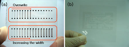 |
| (a) Line images fabricated between platinum dot electrodes on a glass substrate. The upper lines disclose from first to eighth overwriting starting from the left, whereas the bottom lines display changes of the linewidth with fixed overwriting times. The initial linewidth at the outermost left was 170 µm. (b) The direct printing result of a sample circuit diagram on the glass. The overwriting time was five and its transparency was about 85%. (Reprinted with permission from IOP Publishing) |
| The Korean scientists performed the inkjet printing of SWCNTs without any additives. A single inkjet head equipped with a piezoelectric actuation module ejected SWCNT ink droplets onto a glass or a polymer substrate. The solution containing the SWCNTs was centrifuged for 30 minutes to remove large particle residues, and then the supernatant was decanted for use in inkjet printing. The concentration of the ink was approximately 20 µg per milliliter. |
| "As a result of our work, we found that the suitable substrate temperature was about 60°C and hydrophilic treatment of the surface was very desirable" says Han. "In addition, interlaced printing significantly improved the uniform network formation of SWCNTs." |
| Han and his colleagues observed that the network formation of SWCNTs in line patterns played an important role in improving the conductance of the SWCNT line. As expected, repetitive printings on the line make a dense network formation of SWCNTs. Han says that the electrical resistivity was rapidly reduced with the increasing number of overwriting. A sharp increase in both thickness and conductivity was observed during the initial four times overwriting. |
| "We also observed a decrease in resistance in accordance with the increase of the line width" Han explains. "As the width increases from 170 to 1295 µm, its resistance was reduced from 191 to 5.7 kΩ. It is likely that the overlap printing in the contact area of each line width caused a rapid increase in the SWCNT networks. Consequently, the resistance of the line feature of SWCNTs was controllable by changing the line width, the number of overwritings and the overlapping area. Resistance deviation of the lines fabricated with the same conditions (overwriting time and line dimension) was less than 2%, which would be suitable for reproducible manufacturing." |
| Inkjet printing of pure SWCNTs has great potential to make electronic devices on paper, plastic or glass substrates and could become a new alternative for fabricating interconnections in electronic circuits. This SWCNT patterning technique could also potentially be interesting in other areas where CNTs are finding their way into devices such as solar cells or batteries. |
| Han's team is now focused on the fabrication of electronic devices and various electrodes as part of such devices. "In real world applications it is important to make sure that the printed pattern delivers sufficient performance to make the device work" says Han. "Being able to match the printing technique with existing, conventional methods of device fabrication is also important with regard to commercial viability. Consequently, we will begin studying the compatibility with other fabrication processes." |
| Recently, the team has fabricated a wafer scale SWNT gas sensor device using their inkjet printing technique . They are preparing to submit a paper on this accomplishment. |
| The scientists have reported their findings in the February 12, 2008 online edition of Nanotechnology ("Inkjet printing of single-walled carbon nanotubes and electrical characterization of the line pattern"). |
 By
Michael
Berger
– Michael is author of four books by the Royal Society of Chemistry:
Nano-Society: Pushing the Boundaries of Technology (2009),
Nanotechnology: The Future is Tiny (2016),
Nanoengineering: The Skills and Tools Making Technology Invisible (2019), and
Waste not! How Nanotechnologies Can Increase Efficiencies Throughout Society (2025)
Copyright ©
Nanowerk LLC
By
Michael
Berger
– Michael is author of four books by the Royal Society of Chemistry:
Nano-Society: Pushing the Boundaries of Technology (2009),
Nanotechnology: The Future is Tiny (2016),
Nanoengineering: The Skills and Tools Making Technology Invisible (2019), and
Waste not! How Nanotechnologies Can Increase Efficiencies Throughout Society (2025)
Copyright ©
Nanowerk LLC
|

Become a Spotlight guest author! Join our large and growing group of guest contributors. Have you just published a scientific paper or have other exciting developments to share with the nanotechnology community? Here is how to publish on nanowerk.com.
