| Posted: Mar 13, 2008 |
How to pin a drop of water |
| (Nanowerk Spotlight) You have seen the effect: if you splash water on your car it leaves wet areas; if you do this with your freshly polished car the drops just pearl off. Materials scientists are very interested in designing surfaces that allow them to control this effect - called wetting - because it enables them to fabricate things like more comfortable contact lenses, better prosthetics, and self-cleaning materials. The primary measurement to determine wettability is the angle between the solid surface and the surface of a liquid droplet on the solid's surface. For example, a droplet of water on a hydrophobic surface would have a high contact angle, but a liquid spread out on a hydrophilic surface would have a small one. Maintaining the position of a drop of water on a hydrophobic surface (e.g. your newly waxed car) appears to be impossible - it will just move across the surface. |
| Scientists in Israel have managed to fabricate a nanostructured, highly hydrophobic surface that allows them to pin a nearly spherical drop of water in place. A droplet sitting on one class of these substrates did not fall even after the substrate was turned upside-down! An important application for this novel fabrication technique could be as a tool in single-molecule spectroscopy: a water drop, containing molecules to be probed, could be pinned down for an extended time, allowing to spectroscopically probe it for long periods without affecting the properties of molecules, or even just one molecule, dissolved in the water drop. |
| "We found a method to produce substrates that on one hand have very weak interaction with water, but on the other hand can hold a water drop" Dr. Ron Naaman tells Nanowerk. "This sounds like a contradiction in terms, but it happens because there are two length scales involved: On a large scale the substrate is hydrophobic, namely interacts weakly with water; but there are spots on a very small scale (in the nanometer range) that interact strongly with the water. Hence we have a method to keep in place a water drop that is almost spherical." |
| Naaman, the Aryeh and Mintzi Katzman Professor in the Chemical Physics Department at the Weizmann Institute of Science in Israel, notes that in the past there were exotic materials that showed similar properties. His group, however, has developed a relatively simple technique that can be applied on a very simple material – silicon. Naaman, together with postdoc Dr. Adam Winkleman (first author) and students Gilad Gotesman, and Alexander Yoffe, reported their finding in the March 11, 2008 online edition of Nano Letters ("Immobilizing a Drop of Water: Fabricating Highly Hydrophobic Surfaces that Pin Water Droplets"). |
| Rather than a materials engineering approach, this specific study is relevant to the development of bio-analytical methods. There is a growing field of single-molecule spectroscopy dedicated to the detection, analysis and sorting of single molecules. It will not only enable the measurement of mechanical or electrical properties of single molecules – binding forces, forces holding together secondary and tertiary structure of molecules, torque, bond strength, conductivity, etc. – but also the observation of single molecules over time undergoing certain events. |
| One of the challenges in doing this is the difficulty to 'hold' this molecule in place for a long enough time to be studied. Existing methods immobilize molecules on a substrate either by directly linking the probed molecule to the substrate or by immobilizing the molecules by inserting them into surface-tethered lipid vesicles. A downside of these various methods is that they may affect the structure and/or reactivity of the biomolecules that are to be probed. |
| By putting the molecule inside a drop of water and holding the drop in place Naaman and his group solved this problem. |
| The team fabricated arrays of nanometer-sized tips in silicon using both positive and negative photoresist as the mask for creating surfaces by inductively coupled plasma reactive ion etching (ICP-RIE), with features ranging in size from nanometers to micrometers. |
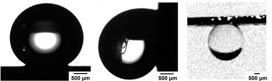 |
| Optical images of a 4 µL drop of water on a substrate from a positive resist. Left: The contact angle for this drop is 147°. Middle: Optical image of a drop of water pinned to the substrate when the tilting angle was ∼90°; gravity deforms the drop shape, but the drop does not move along the surface. Right: Drop suspended upside-down by manually rotating the substrate 180°. (Reprinted with permission from American Chemical Society) |
| "Our tips were fabricated with features over 2 orders of magnitude, where the smallest features, the diameter of the tip, were as small as 15 nm" says Naaman. "Upon silanization of these surfaces with hydrophobic monolayers the substrates fabricated from the positive photoresist yielded contact angles >140° and as large as 162°. The tilting angle was defined as the angle at which the drop falls from the surface. When a water droplet was positioned on the surface and the substrate was tilted slowly, the droplet did not roll or slide even for angles up to 90°. For those substrates, the drop could also be flipped 180° and suspended upside-down." |
| The fabrication process of the arrays of nanoscale tips is based on either a positive or negative photoresist that was spun-cast onto a silicon wafer. "Both the positive and negative substrates were exposed through a chromium photomask, and the resists were developed to yield either an array of square wells or square posts, respectively" explains Naaman. "Unlike previously reported methods for fabricating nanometer-size tips, we use the patterned photoresist directly as the mask for the reactive ion etching procedure and not a silicon oxide or nitride layer, as is more common." |
| Using the photoresist as the etching mask simplifies the processing of the silicon substrate by eliminating at least one step. The main requirement for the photoresists was that they should not degrade during the RIE process. Naaman points out that both the positive and negative photoresists survive the RIE process, and the photoresists had to be removed by sonication in organic solvents to yield the array of nm tips. |
| The resulting substrates have ordered structures on the size scale of of tens to hundreds of nanometers evenly spaced by a few micrometers plus a surface roughness of a few nanometers due to the etching process. Naaman says that this type of substrate is different from former cases that demonstrated both high contact angle and large tilting angles. "The common feature of all systems in which pinning of water drops is observed, together with high contact angle, is the presence of regions with pores that could possibly trap air that is isolated from the atmosphere. It seems that the small degree of pitting is crucial to the adhesion." |
| The Weizmann Institute scientists describe the advantages of their process are as follows: |
| 1) it uses standard chemical processes (photolithography, RIE, and silanization) and materials (silicon wafers); |
| 2) it makes surfaces over relatively large areas (>1 cm2); and |
| 3) it yields very hydrophobic surfaces that allow for ease of handling of substrates after applying a water drop without loss of the drop. |
| "The drawbacks of our substrates are that a clean room facility is required for fabrication, the exact nature and features of the surface are very sensitive, and much care must be taken to achieve reproducibility" says Naaman. |
| It appears that the specific surfaces that his group produced also have some special properties when serving as photocathodes. The group is exploring these properties right now. |
 By
Michael
Berger
– Michael is author of four books by the Royal Society of Chemistry:
Nano-Society: Pushing the Boundaries of Technology (2009),
Nanotechnology: The Future is Tiny (2016),
Nanoengineering: The Skills and Tools Making Technology Invisible (2019), and
Waste not! How Nanotechnologies Can Increase Efficiencies Throughout Society (2025)
Copyright ©
Nanowerk LLC
By
Michael
Berger
– Michael is author of four books by the Royal Society of Chemistry:
Nano-Society: Pushing the Boundaries of Technology (2009),
Nanotechnology: The Future is Tiny (2016),
Nanoengineering: The Skills and Tools Making Technology Invisible (2019), and
Waste not! How Nanotechnologies Can Increase Efficiencies Throughout Society (2025)
Copyright ©
Nanowerk LLC
|

Become a Spotlight guest author! Join our large and growing group of guest contributors. Have you just published a scientific paper or have other exciting developments to share with the nanotechnology community? Here is how to publish on nanowerk.com.
