| Posted: Feb 23, 2018 |
Molecular printing with light-actuated pens |
| (Nanowerk Spotlight) The past two decades have witnessed the evolution of advanced physical probe-based nanolithography techniques for molecular printing. Dip-Pen Nanolithography (DPN) for instance is a scanning probe lithography technique in which the tip of an atomic force microscope (AFM) is used to 'write' molecules directly onto a substrate, allowing nanostructured surface patterning on scales of under 100 nm. DPN is the nanotechnology analog of the dip pen where the AFM tip acts as a 'pen', which is then dipped into a molecular 'ink' (i.e. coated with a chemical compound or mixture), and then used to write functional nanoscale patterns by putting it in contact with a substrate, the 'paper'. |
| To scale these techniques up from a single pen to millions, the cantilever conventionally found in AFM-based systems is replaced with an array of polymer pens that rest on an elastomeric film on a rigid backing substrate, providing large-scale, high-resolution printing at low cost. |
| "In order for techniques using arrays of cantilever-free polymer pens to be a general nanopatterning platform, there needs to be a way to direct the action of each pen individually; and this has been a key challenge: multiplexing," YuHuang Wang, a professor in the Department of Chemistry and Biochemistry at the University of Maryland, tells Nanowerk. "For these techniques to be a general nanopatterning platform, there needs to be a way to direct the action of each pen individually. This has been a dream goal that had been actively sought-after for more than two decades." |
| Wang and his team, together with collaborators from Boston University, have made important progress in addressing this challenge by fabricating pens that can be photo-actuated to perform molecular printing. They have reported their findings in Advanced Materials ("Photoactuated Pens for Molecular Printing"). |
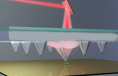 |
| Schematic illustration of a photoactuated pen within an array. The pyramidal pen and the backing layer are made of PDMS–CNT composites which can locally expand upon light irradiation. When light is on, the local deformation moves the pen out of plane into contact with the substrate so that ink material is transferred to the substrate. This actuation is reversible and occurs locally. (Reprinted with permission by Wiley-VCH Verlag) |
| This work is the first demonstration of photo-actuated polymer pens for molecular printing and represents an important step in the field of scalable nanofabrication. It paves the way for dynamic actuation of individual pens, making it possible to realize patterning and printing molecules or other soft materials such as polymers or biomaterials at high resolution and low cost. |
| There have been previous efforts trying to achieve multiplexing, but all require the pen array to be very complex, which compromises the impact of the patterning approach. For polymer pen lithography, efforts to multiplex actuation using electrically-driven thermal actuation and pneumatic systems have not been scaled to massive arrays due to the complexity that they require to be built into the pen array. |
| In this work, the researchers exploited large photo-actuation effects from polydimethylsiloxane-carbon nanotube composites. They used this material to synthesize the pens for their printing arrays. They show that a selected group of pens can be expanded by more than three micrometers out of plane (representing ∼1% strain of the supporting PDMS film). |
| This actuation is rapid, energy efficient, and fully reversible. Importantly, the actuation occurs locally; pens outside the illumination area are not actuated and thus do not print, making it possible to achieve actuation on specific pens in a large array. |
| "Although we knew that localized heating can occur as nanotubes absorb light, it is completely unexpected and amazing that this effect alone is large enough to drive the pens to perform molecular printing," says Wang. |
| "Since light can be easily directed using equipment equivalent to common projectors, this makes the pen arrays simple and effective," notes Zhongjie Huang, a postdoctoral researcher in Wang's group and the paper's first author. "Our work shows the way for the arbitrary control of individual pens in a massively parallel array with light." |
| While the team has successfully actuated a selected group of pens, the next goal is to achieve the independent control of each single pen. It will require that the illuminated area is commensurate with the size of an individual pen and that the light directed to each pen can be controlled independently. |
| "Digital micromirror devices, which have been successfully incorporated in beam pen lithography, can likely fill this role as they can direct millions of beams of light to microscale domains," concludes Wang. "Further, efficient independent actuation will also require a sophisticated investigation including an optimization of optical power, pen-to-pen pitch, and learning how to mitigate crosstalk between pens." |
 By
Michael
Berger
– Michael is author of four books by the Royal Society of Chemistry:
Nano-Society: Pushing the Boundaries of Technology (2009),
Nanotechnology: The Future is Tiny (2016),
Nanoengineering: The Skills and Tools Making Technology Invisible (2019), and
Waste not! How Nanotechnologies Can Increase Efficiencies Throughout Society (2025)
Copyright ©
Nanowerk LLC
By
Michael
Berger
– Michael is author of four books by the Royal Society of Chemistry:
Nano-Society: Pushing the Boundaries of Technology (2009),
Nanotechnology: The Future is Tiny (2016),
Nanoengineering: The Skills and Tools Making Technology Invisible (2019), and
Waste not! How Nanotechnologies Can Increase Efficiencies Throughout Society (2025)
Copyright ©
Nanowerk LLC
|

Become a Spotlight guest author! Join our large and growing group of guest contributors. Have you just published a scientific paper or have other exciting developments to share with the nanotechnology community? Here is how to publish on nanowerk.com. |
