| Posted: Jul 28, 2008 |
First prototype of an integrated optoelectronic SWCNT device |
| (Nanowerk Spotlight) Transparent conductive coatings pervade modern technology and they are a critical component of optoelectronic devices. Today, the most widely used standard coating in nearly all flat panel displays and microdisplays is indium tin oxide (ITO). As indium becomes increasingly scarce and expensive, the search for novel transparent electrode materials with good stability, high transparency and excellent conductivity has become a crucial goal for optoelectronic researchers. |
| There are strong and successful efforts from several research groups around the world to develop optoelectronic devices on the basis of individual single-walled carbon nanotubes (SWCNTs). This development is of great scientific interest, although there are major challenges in finding technologically feasible ways to assemble the individual nanotube devices into functioning electronic circuits with a high level of integration. |
| One possible solution is to use networks of entangled SWCNTs that have been grown into continuous, semi-transparent thin film. Such SWCNT thin films are easy to cast from SWCNT solution, they can be lithographically patterned, and the preparation of such films requires only micrograms of SWCNT material, thus this is a low cost technology. |
| "We use the suspended SWCNT thin film technology to demonstrate the first prototype of an integrated optoelectronic SWCNT device, a SWCNT optocoupler in which a SWCNT emitter and a SWCNT detector couple two electrical circuits by the transmission of a signal through the optical channel," Dr. Robert Haddon tells Nanowerk. |
| Haddon, Distinguished Professor, Chemical and Environmental Engineering, and Director of the Center for Nanoscale Science and Engineering at the University of California, Riverside, has just published a new paper that reflects his group's continuing efforts to develop optoelectronics on the basis of single-walled carbon nanotube (SWCNT) thin film technology ("Single-Walled Carbon Nanotube Thin Film Emitter-Detector Integrated Optoelectronic Device"). |
| In previous work, Haddon's team had demonstrated that the photoresponse of SWCNT thin film is enhanced by many orders of magnitude when it is suspended in vacuum between electrical contacts ("Bolometric Infrared Photoresponse of Suspended Single-Walled Carbon Nanotube Films"). |
| "This enhancement originates from the ability of SWCNTs to absorb infrared light more strongly than conventional semiconductors and to efficiently convert the absorbed energy into an electrical signal through the bolometric effect – the heating of the SWCNT film under infrared radiation changes its electrical resistance, which strongly depends on temperature," Haddon explains. "This strong photoresponse can be utilized to manufacture a new type of infrared bolometric detector." |
| In their recent Nano Letters publication, Haddon's team demonstrated the first prototype of a SWCNT integrated optoelectronic device in which they introduced a SWCNT thin film emitter which operates together with a SWCNT thin film detector to transfer a signal between two electrical circuits through the optical channel without electrical coupling thus making an optocoupler; a device widely utilized in conventional semiconductor-based optoelectronics. |
| To prepare their optocoupler device, the UC Riverside team utilized free-standing SWCNT films of electric arc produced and purified SWCNTs prepared by vacuum filtration. |
| "We made the detector by suspending a narrow ribbon of SWCNT film across the opening of a sapphire ring; a second sapphire ring was used to support a SWCNT thin film emitter in a similar way" Haddon explains the procedure. "The two sapphire rings were attached by thermally conducting adhesive paste back to back so the SWCNT emitter and detector were facing each other at a separation of 2.0 mm. The dimensions (length × width × thickness) of the SWCNT detector and emitter were 1 mm long x 0.24 mm wide x 100 nm thick and 2.2 mm x 0.64 mm x 150 nm, respectively. The sapphire rings were mechanically and thermally attached to the coldfinger of a continuous flow optical cryostat with the sample space maintained in vacuum." |
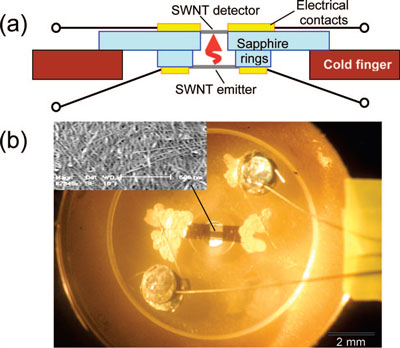 |
| (a) Schematic of the SWCNT optocoupler: SWCNT thin film emitter and detector are mounted face-to-face on two sapphire rings so the radiation from SWCNT emitter can be sensed by the detector. (b) Optical microscope image of the SWCNT optocoupler. Both SWCNT emitter and detector films are ultrathin and semitransparent, so the narrow strip of SWCNT detector (on the back) can be seen through the SWCNT emitter film (in front). Inset: SEM image of the SWCNT film. (Reprinted with permission from American Chemical Society) |
| Applications based on SWCNT thin film technology are now recognized as a near term alternative to the development of nanoelectronics based on individual SWCNTs. |
| Haddon says that he envisions that SWCNT thin films will become a new advanced optoelectronic material which can be applied to the manufacture of high density focal plane arrays of infrared detectors for thermal imaging, infrared astronomy and medical imaging. "The SWCNT-based integrated optoelectronic devices such as optocoupler potentially may find application when a higher level of integration is required as in the development of 3D-electronics where optical communication between different 2D-layers is needed," he adds. |
| Among research groups around the world, SWCNT thin film technology is utilized to substitute ITO as a highly transparent conducting coating for large area optoelectronics. Additional projects in Haddon's lab include development of gas sensors and a new type of fuel cells on the basis of SWCNT thin films. |
| Haddon points out that SWCNT thin film technology still requires significant efforts in order to bring it to practice. He lists reducing the size of individual elements by utilizing lithography, optimizing SWCNT device performance, and especially increasing the speed of operations as the Important issues that need to be tackled. |
| "Further development of the SWCNT thin film optocoupler will incorporate thin film photolithography which would allow the manufacture of multichannel arrays of SWCNT-based optocouplers with pixel size of 30-20 µm, which is comparable to current focal plane array technology," he says. "Such size decrease would permit a significant reduction of the power per individual optocoupler and a significantly faster response time which is an important characteristic of the optocoupler performance." |
 By
Michael
Berger
– Michael is author of four books by the Royal Society of Chemistry:
Nano-Society: Pushing the Boundaries of Technology (2009),
Nanotechnology: The Future is Tiny (2016),
Nanoengineering: The Skills and Tools Making Technology Invisible (2019), and
Waste not! How Nanotechnologies Can Increase Efficiencies Throughout Society (2025)
Copyright ©
Nanowerk LLC
By
Michael
Berger
– Michael is author of four books by the Royal Society of Chemistry:
Nano-Society: Pushing the Boundaries of Technology (2009),
Nanotechnology: The Future is Tiny (2016),
Nanoengineering: The Skills and Tools Making Technology Invisible (2019), and
Waste not! How Nanotechnologies Can Increase Efficiencies Throughout Society (2025)
Copyright ©
Nanowerk LLC
|

Become a Spotlight guest author! Join our large and growing group of guest contributors. Have you just published a scientific paper or have other exciting developments to share with the nanotechnology community? Here is how to publish on nanowerk.com. |
