Showing Spotlights 121 - 128 of 332 in category All (newest first):
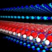
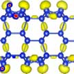 In the past few years, monolayer and multilayer silicenes have been successfully grown on various metal substrates. Unfortunately, silicene on metal substrate generally exhibits metallic or semi-metallic character without a bandgap, and thus cannot be used as adsorption layer of photovoltaic materials. A new comprehensive investigation of multilayer silicene by means of ab initio swarm-intelligence structure-searching method predicts that tri-layer silicene is an ideal candidate for high-efficiency photovoltaic absorbers.
Oct 15th, 2018
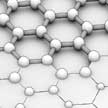 A new study on worldwide graphene production shows unequivocally that the quality of the graphene produced in the world today is rather poor, not optimal for most applications, and most companies are producing graphite microplatelets. This is possibly the main reason for the slow development of graphene applications, which usually require a customized solution in terms of graphene properties. A conclusion that sounds even more damming is that this extensive study of graphene production worldwide indicates that there is almost no high quality graphene, as defined by ISO, in the market yet.
Oct 9th, 2018
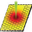
 Researchers have developed a way to achieve an ultra-high bioelectric signal from human embryonic stem cells using direct current-voltage measurements facilitated by few-layered 2D molybdenum disulfide sheets. This method, which produces cell signals 2 orders of magnitude higher than previous electrical-based detection methods, paves the way for the development of a broadly applicable, fast, and damage-free stem cell detection method capable of identifying pluripotency with virtually any complementary metal-oxide-semiconductor circuits.
Sep 17th, 2018
 Black phosphorus (BP or phosphorene), a novel two-dimensional semiconducting material, has gained tremendous attention because of its intriguing properties, such as ON/OFF ratio, high carrier mobility, and tunable direct band. However, a fundamental obstacle hindering practical applications is the lack of stability under ambient conditions. Now researchers demonstrated both excellent photoelectrochemical performance and significantly improved stability based on tin monosulfide nanosheets. These findings hold great potential for practical applications of phosphorene analogue nanomaterials-based devices.
Sep 13th, 2018
 Graphene bioelectronics has become a ground-breaking field that offers exciting opportunities for developing new kinds of sensors capable of establishing outstanding interfaces with soft tissue. Graphene-based transistors, as well as electrode arrays, have emerged as a special group of biosensors with their own peculiarities, advantages and drawbacks. A new review present sa comprehensive overview of the use of graphene for bioelectronics applications; specifically the focus is on interfacing graphene-based devices with electrogenic cells, such as cardiac and neuronal cells.
Sep 3rd, 2018
 Researchers have developed an all-optical lithographic technique called 'optothermoplasmonic nanolithography' (OTNL) to achieve high-throughput, versatile, and maskless patterning of different atomic layers. Taking graphene and molybdenum disulfide monolayers as examples, the team shows that both thermal oxidation and sublimation in the light-directed temperature field can lead to direct etching of the atomic layers. They further demonstrates programmable patterning of 2D materials into complex and large-scale nanostructures by steering the laser beam.
Aug 14th, 2018
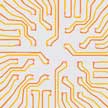
 Traditional CMOS technology cannot be directly merged with graphene applications. Photo- and electron-based lithographies, which are the main processess in today's semiconductor industry, requires use of polymers and harsh liquids that can drastically alter the initial properties of graphene. Thus graphene requires the development of novel processing technologies.
A international team of researchers now has developed a method for direct, on-the-fly reconstruction of graphene properties.
Traditional CMOS technology cannot be directly merged with graphene applications. Photo- and electron-based lithographies, which are the main processess in today's semiconductor industry, requires use of polymers and harsh liquids that can drastically alter the initial properties of graphene. Thus graphene requires the development of novel processing technologies.
A international team of researchers now has developed a method for direct, on-the-fly reconstruction of graphene properties.
Jul 30th, 2018
 An international team of researchers has discovered a new mechanism for controlling electronic devices using molecules. The ferroelectric ordering of polar molecules attached to the edge of graphene can be toggle-switched by an electrostatic gate and can be used for memory devices and sensors. For this work, the team sandwiched graphene layers in hexagonal boron nitride crystals. The trick is to control the edge chemistry. The researchers attached different atoms to the graphene edges, before exposing them to water vapor and other polar molecules.
Jul 27th, 2018
 Subscribe to our Nanotechnology Spotlight feed