Showing Spotlights 169 - 176 of 252 in category All (newest first):
 A memristor is a two-terminal electronic device whose conductance can be precisely modulated by charge or flux through it. It has the special property that its resistance can be programmed (resistor) and subsequently remains stored (memory). It is thought memristors - with the ability to 'remember' the total electronic charge that passes through them - will be of greatest benefit when they can act like synapses within electronic circuits, mimicking the complex network of neurons present in the brain, enabling our own ability to perceive, think and remember. Researchers have now analyzed in unprecedented detail the physical and chemical properties of an electronic device that computer engineers hope will transform computing.
May 16th, 2011
 Ink-jet printing of metal nanoparticles for conductive metal patterns has attracted great interest as an alternative to expensive fabrication techniques like vapor deposition. The bulk of the research in this area focuses on printing metal nanoparticle suspensions (metallic ink) for metallization. Printing conductive features by metallic nanoparticle inks must be followed by an additional step of sintering, usually achieved by heating to elevated temperatures. In this step, the nanoparticles composing the pattern will coalesce to form a continuous electrical contact. In new work, researchers have now demonstrated a new conductive ink that won't require a post printing sintering step. It is achieved by the addition of a latent sintering agent that gets into action after the printing step. Once the solvent evaporates, the sintering agent concentration increases, leading to the spontaneous sintering of the nanoparticles.
Apr 18th, 2011
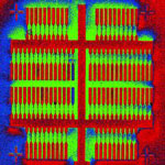 The commercial realization of carbon nanotube-based electronic devices and their integration into the existing silicon-based processor technologies is still hampered by the inability to scale up the - currently lab-based - fabrication processes to manufacture a large number of devices on a single chip. The fundamental issue of carbon nanotube device fabrication still remains the biggest challenge for effective commercialization of nanotube electronics. In a further step towards large-scale integration of single-walled carbon nanotubes (SWCNTs) into complex functional electronic circuits, researchers have now combined a previously developed dielectrophoretic deposition approach with SWCNT sorting using density gradient ultracentrifugation, ensuring high purity of SWCNTs in suspension and consequently in the assembled devices.
Mar 22nd, 2011
 Although organic semiconductor materials cannot yet be packed as densely as state-of-the-art silicon chips, they require less power, cost less and do things silicon devices cannot: bend and fold, for example. Once perfected, organic semiconductors will permit the construction of low-cost, spray-on solar cells and even spray-on video displays. Notwithstanding tremendous progress in the area of organic electronics, several major challenges still exist. To address these challenges, researchers have combined organic electronics with nanoelectronics and developed the first 2D crystal of organic semiconductors on the millimeter scale, the thickness of which is only a single molecular layer, but with perfect long-ranged crystalline order.
Mar 15th, 2011
 Printed electronics has its origins in conductive patterns printed as part of conventional electronics, forming flexible keyboards, antennas and so on. Then came fully printed testers on batteries, electronic skin patches and other devices made entirely by printing, including batteries and displays. A clear next step has been to modernise static print with the e-reader and the talking poster with animated, light emitting display and solar power. These are partly or almost wholly printed, with a clear roadmap to making them lower cost and more reliable and flexible by using printing more fully in their manufacture in future. However, we now see printed electronics and electrics certain to penetrate far more applications than anyone realised.
Feb 15th, 2011
 One of the many fascinating concepts in nanotechnology is the vision of molecular electronics where researchers are investigating nanostructured materials to build electronics from individual molecules. If realized, the shift in size from even the most densely packed computer chip today would be staggering. Molecular electronics aims at the fundamental understanding of charge transport through molecules and is motivated by the vision of molecular circuits to enable miniscule, powerful and energy efficient computers. A research team in Germany has now demonstrated that rigidly wired molecules can emit light under voltage bias. This result is important for fundamental science but it also adds to the molecular electronics vision an optoelectronic component, i.e. the development of optoelectronic components on the basis of single molecules.
Nov 29th, 2010
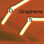 So far, there have been no research reports on a graphene-based transistor amplifier and investigations of its in-field controllability for analog, mixed-signal, and radio-frequency applications. Previous work on graphene transistors has largely focused on frequency multiplication near the Dirac point in graphene current-voltage characteristic. But now, a team of researchers has demonstrated the first triple-mode graphene amplifier. They have shown experimentally that by leveraging the ambipolarity of charge transport in graphene, the amplifier can be configured in the common-source, common-drain, or frequency multiplication mode of operation by changing the gate bias. This is the first demonstration of a single-transistor amplifier that can be tuned between different modes of operation using a single three-terminal transistor. Moreover, during its operation, the graphene amplifier was configured in-field to switch between the different modes. The result marks another important step toward graphene applications in electronics.
Oct 11th, 2010
 Zinc oxide is considered a workhorse of technological development exhibiting excellent electrical, optical, and chemical properties with a broad range of applications as semiconductors, in optical devices, piezoelectric devices, surface acoustic wave devices, sensors, transparent electrodes, solar cells, antibacterial activity etc. Thin films or nanoscale coating of ZnO nanoparticles are viewed with great interest for their many potential applications as substrates for functional coatings. Researchers in Taiwan have now shown, for the first time, that they can directly grow vertically aligned, highly crystalline and defect-free single-crystalline zinc oxide nanorods and nanoneedles on paper.
Oct 6th, 2010
 Subscribe to our Nanotechnology Spotlight feed