| Posted: Aug 04, 2009 | |
Textured network devices to solve fundamental problems with CNT nanoelectronics |
|
| (Nanowerk Spotlight) The charge-carrier mobility is a crucial issue when considering the use of carbon nanotubes and other materials for nanoelectronics applications. Modern electronics relies on field effect transistors (FET) to amplify or switch electronic signals. Semiconducting carbon nanotubes – since their conductance can be changed by applying a voltage on a third electrode – can act like a switch and therefore are considered a promising material for future FETs. | |
| The degree of mobility of a semiconductor, i.e. how well it conducts, is crucial to the effectiveness of nanoelectronic devices. Mobility determines the carrier velocity, and hence switching speed, in FETs. Researchers have determined that the theoretical mobility of an individual single-walled carbon nanotube (SWCNT) is higher than 100,000 cm2/Vs (centimeters squared per volt-second) at room temperature, higher than any other known semiconductor. By comparison, the typical electron mobility for silicon at room temperature is 1,400 cm2/Vs. | |
| However, practical applications would require massive manufacturing of large scale nanoelectronic devices. Despite progress being made with integrating individual nanotubes in lab environments (see for instance: "Carbon nanotubes to the rescue of Moore's law"), many of today's nanomanufacturing techniques for nanoelectronic devices rely on the use of 'carbon nanotube network films' comprised of multiple carbon nanotubes (CNTs). | |
| The major problem here is that the electronic properties of CNT network films are usually very poor. For example, the mobility of CNT network films comprised of randomly-oriented CNTs is usually about 5 cm2/Vs, which is much worse than silicon and is actually similar to that of organic conductors. | |
| In addition, since CNT network films are comprised of both metallic and semiconducting CNTs, transistors based on CNT network films do not turn off, which can be a problematic for integrated circuit applications. | |
| These are the fundamental problems of CNT network-based devices, which have been holding back any practical applications of CNT-network based devices. | |
| Researchers in South Korea have now developed a powerful strategy to solve these fundamental problems simply by controlling the connectivity of SWCNT/nanowire networks. They utilized a 'surface-programmed assembly' technique to create CNT network films comprised of aligned CNTs. | |
 |
|
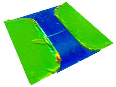
| 3D image of a device based on aligned CNT networks. The image shows two electrodes (wide green regions) connected by a 100nm-wide channel comprised of aligned CNT networks (thin green line) on the SiO2 substrate (wide blue regions). (Image: Dr. Seunghun Hong, Seoul National University). | |
| "We found that we can improve the transistor behavior and mobility of CNT network films simply by aligning CNTs in the network films, which effectively enhances their serial connectivity" Seunghun Hong, an associate professor of physics at Seoul National University, tells Nanowerk. "For example, we can achieve a mobility as large as 180 cm2/Vs by aligning CNTs in 100nm wide channels. Using this strategy, we significantly improved the yield of SWCNT network-based FETs with a large on–off ratio without removing metallic SWCNTs" | |
| Hong and his team have reported their findings in a recent paper in Small ("'Textured' Network Devices: Overcoming Fundamental Limitations of Nanotube/Nanowire Network-Based Devices"). | |
| "We could fabricate high-performance FETs with high yield of about 88% using textured network channels while maintaining high current level," Hong explains. "Significantly, both experiments and simulations showed that the textured network channels enhance conductivity and mobility with reduced line width, which is a completely opposite behavior to randomly oriented SWCNT networks or even conventional silicon-based devices. It indicates that this strategy can be an ultimate solution to solve the fundamental limitations for scaling down nanoelectronic devices." | |
 |
|
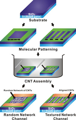
| Schematic diagram depicting the fabrication procedure of FETs based on random or textured SWCNT network channels. (Reprinted with permission from Wiley-VCH Verlag) | |
| The basic procedure to prepare devices with random or textured SWCNT network channels is similar to that reported by Hong and collaborators previously in Nature Nanotechnology ("Linker-free directed assembly of high-performance integrated devices based on nanotubes and nanowires"): They patterned a self-assembled monolayer with non-polar terminal groups onto a silicon dioxide surface using photolithography or e-beam lithography. When the substrate was placed in the SWCNT suspension, the nanotubes were selectively adsorbed onto bare silicon dioxide regions up to a full monolayer (since SWCNTs show strong affinity to most bare surfaces – for example, gold, silicon dioxide, glass, silicon and aluminum – this affinity can be used as a means to direct SWCNT assembly). | |
| Hong and his colleagues are now working on applying their method using purified CNTs with uniform properties, which should allow them to mass-produce uniform arrays of high-performance CNT network-based devices. Actually, they have developed high-performance sensors based on this strategy but the manuscript on these findings,including the results, are currently under review. | |
 By
Michael
Berger
– Michael is author of three books by the Royal Society of Chemistry:
Nano-Society: Pushing the Boundaries of Technology,
Nanotechnology: The Future is Tiny, and
Nanoengineering: The Skills and Tools Making Technology Invisible
Copyright ©
Nanowerk LLC
By
Michael
Berger
– Michael is author of three books by the Royal Society of Chemistry:
Nano-Society: Pushing the Boundaries of Technology,
Nanotechnology: The Future is Tiny, and
Nanoengineering: The Skills and Tools Making Technology Invisible
Copyright ©
Nanowerk LLC
|
|
|
Become a Spotlight guest author! Join our large and growing group of guest contributors. Have you just published a scientific paper or have other exciting developments to share with the nanotechnology community? Here is how to publish on nanowerk.com. |
|