| Posted: Jul 27, 2015 | |
Suppressing flicker noise in graphene boron nitride heterostructure field-effect transistors |
|
| (Nanowerk Spotlight) The low-frequency 1/f noise (sometimes called pink noise or flicker noise), which is usually found at frequencies below 100 kHz, is a ubiquitous phenomenon found in many physical, biological and even economic systems – fluctuations of the sea level; intensity in a music recording; human heart rates; or electrical currents in semiconductor devices. | |
| This flicker noise is a crucial performance metric in many devices because it limits the sensitivity and selectivity of all the sensors that rely on an electrical response. This also includes future electronic applications of graphene that do not seriously suffer from the absence of an energy band gap but rely on graphene’s high electron mobility, thermal conductivity, saturation velocity, and a possibility of tuning the charge carrier concentration. These applications include analog electronics, high-frequency communications, THz plasmonic devices and sensor. For all these applications, the low-frequency electronic 1/f noise is a critical performance metric. | |
| "The low-frequency noise is responsible for the dominant contribution to the phase noise of the communication systems even when they operate at much higher carrier frequency," Alexander A. Balandin, professor of electrical and computer engineering at UC Riverside (UCR), explains to Nanowerk. "It also limits sensitivity and selectivity of chemical and biological sensors." | |
| The noise level in devices with graphene and other two-dimensional (2D) materials has to be reduced in order to enable their practical applications. It will not be possible to build graphene-based communication systems or detectors until the noise spectral density is decreased to the level comparable with the conventional state-of-the-art transistors. | |
| Researchers are looking for methods suitable for noise reduction in these new 2D materials systems. A research team led by Balandin has recently demonstrated that the electronic noise in graphene devices can be strongly suppressed if a graphene channel is encased between two layers of hexagonal boron nitride (h-BN) (see Figure 1). | |
 |
|
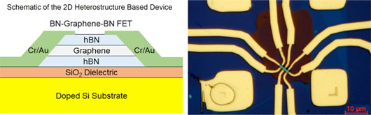
| Figure 1: Schematics of h-BN-graphene-h-BN heterostructure field-effect transistor (HFET). Note the structure the 'one-dimensional' contact to the fully encapsulated graphene layer (left panel). Optical microscopy image of a representative graphene encapsulated HFET (right panel). (Image: Professor Alexander A. Balandin and Maxim Stolyarov, Nano-Device Laboratory, University of California – Riverside) | |
| The team published their findings in the July 14, 2015 online edition of Applied Physics Letters ("Suppression of 1/f noise in near-ballistic h-BN-graphene-h-BN heterostructure field-effect transistors"). The members of the research team included Maxim Stolyarov, Graduate Research Assistant, Dr. Guanxiong Liu, Postdoctoral Associate in Professor Balandin's Nano-Device Laboratory (NDL), and Dr. Sergey Rumyantsev and Professor Michael Shur of the Rensselaer Polytechnic Institute (RPI). | |
| Specifically, they report on the low-frequency noise in the hexagonal boron nitride-graphene-boron nitride (h-BN-G-h-BN) heterostructure field-effect transistors (HFETs) on Si/SiO2 substrates. | |
| The heterostructure h-BN-G-h-BN transistors had very high charge carrier mobility in the range from ∼30000 to ∼36000 cm2/Vs at room temperature. | |
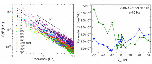
| "Our measurements established that the noise spectral density normalized to the channel area in such devices can be suppressed by an order of magnitude as compared to 'conventional' non-encapsulated graphene devices on silicon substrates,"says Balandin (see Figure 2). "We attributed the physical mechanism of noise suppression to screening of the charge carriers in the channel from traps in SiO2 gate dielectric and surface defects." | |
 |
|
| Figure 2: Normalized noise spectrum density in h-BN-graphene-h-BN heterostructure field-effect transistor (HFET) as a function of frequency for several values of the back-gate bias (left panel). The noise parameter β, which defines 1/f noise level in 2D channels plotted as a function of gate bias for two representative devices (right panel). (Image: Professor Alexander A. Balandin and Maxim A. Stolyarov, Nano-Device Laboratory, University of California – Riverside) | |
| There have been a number of papers published on 1/f noise in graphene on conventional silicon and silicon oxide substrates. By researching this issue, scientists realized that, although both the graphene layer itself and metal contacts contribute to the 1/f noise, the dominant contribution mostly comes from the graphene channel itself. | |
| "The key for noise suppression is in screening graphene channels from defects and scattering centers in the gate dielectric, substrate and surface," Balandin points out. | |
| The present paper is the first demonstration of such approach. The team shows that in the design of heterostructure h-BN-graphene-h-BN field-effect transistors, the h-BN layers help to screen the electrical current in graphene channel from defects in surrounding materials. | |
| "It was known before that boron nitride encapsulation of graphene allows one to substantially increase the electron mobility," notes Balandin. "With the mobility of above 30,000 cm2/Vs even micrometer-scale devices operate in near ballistic regime at room temperature. In our work, we demonstrated that in addition to increased mobility such heterostructure devices also have strongly suppressed noise level." | |
| "This is important for practical applications," he adds. | |
| In order to quantify noise level in devices with the channels implemented with 2D materials such as graphene or MoS2, the UCR-RPI team introduced a new metric suitable for 2D materials. It is the noise spectral density normalized to the device channel area, denoted as β parameter β=(SI/I2)(W × L), where SI is the noise spectral density, I is the electrical current in the channel, W is the channel width and L is the channel length. | |
| According to the researchers, the new figure of merit was required because traditional noise characteristics were introduced for bulk materials. | |
| "Our next task will be to accurately benchmark 2D materials and devices against noise level in conventional silicon complementary metal-oxide-semiconductor (CMOS) transistors and field-effect transistors (FETs) made of other semiconductors," concludes Balandin. "After that, we will understand better what improvements in quality of 2D materials and design of 2D devices are needed in order for them to compete with conventional semiconductors." | |
| The work at UC Riverside was supported, in part, by the Semiconductor Research Corporation (SRC) and Defense Advanced Research Project Agency (DARPA) through STARnet Center for Function Accelerated nanoMaterial Engineering (FAME) and by the National Science Foundation (NSF) project Graphene Circuits for Analog, Mixed-Signal, and RF Applications. | |
 By
Michael
Berger
– Michael is author of three books by the Royal Society of Chemistry:
Nano-Society: Pushing the Boundaries of Technology,
Nanotechnology: The Future is Tiny, and
Nanoengineering: The Skills and Tools Making Technology Invisible
Copyright ©
Nanowerk LLC
By
Michael
Berger
– Michael is author of three books by the Royal Society of Chemistry:
Nano-Society: Pushing the Boundaries of Technology,
Nanotechnology: The Future is Tiny, and
Nanoengineering: The Skills and Tools Making Technology Invisible
Copyright ©
Nanowerk LLC
|
|
|
Become a Spotlight guest author! Join our large and growing group of guest contributors. Have you just published a scientific paper or have other exciting developments to share with the nanotechnology community? Here is how to publish on nanowerk.com. |
|