| Posted: Mar 02, 2016 | |
Writing nanotubes with a nano fountain pen |
|
| (Nanowerk Spotlight) One of the fundamental challenges in the development of nanoelectromechanical systems (NEMS) – and of nanotube- and nanowire-based devices in general – is the large-scale controlled placement of molecular sized building blocks on a substrate. | |
| The ability to effectively place molecules at will so that they can be rapidly organized into functional components is a core requirement of many nanotechnology applications, components and functional devices. | |
| In new work, an international team of researchers describes the drawing and Raman characterization procedure developed for placing single-walled carbon nanotubes (SWCNTs), proof of SWCNT alignment, optimization of the drawing parameters, and the subsequent placement in predefined lithographic structures for the demonstration of electrical conductivity. | |
| The findings have been published in the January 20, 2016 online edition of Nano Letters ("Nanodrawing of Aligned Single Carbon Nanotubes with a Nanopen"). | |
| In essence, the team developed a simple nano pen for drawing and placing aligned single or multiple rod like molecules nanometrically. This is exemplified in the paper by a focus on carbon nanotubes, considered widely as a critical element in molecular electronics. | |
 |
|
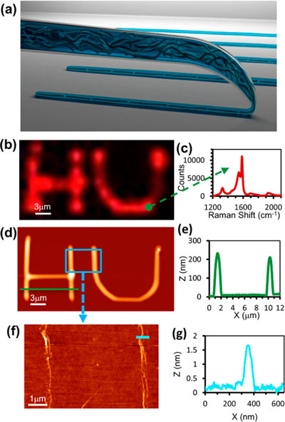
| Controlled direct drawing of SWCNTs on SiO2. (a) A diagrammatic representation of the drawing process. The SWCNT alignment occurs by capillary forces in the direction of drawing. (b) Raman mapping of the written structure of the G+ band together with (c) a Raman spectrum at a point in this image. (d) AFM of the written structure before washing with (e) a line scan of a particular location. The height of the drawing is 200-250 nm, and the line width is 600-800 nm. (f) AFM of a portion of the written structure that has been washed after 4 days of drying, with (g) a line scan at a particular location. After washing only the SWCNTs remained on the substrate with the associated surfactant and solution being washed away. The height of the drawn structure is between 0.8 and 2.9 nm. (Reprinted with permission by American Chemical Society) | |
| "The basis of the methodology, which is the use of capillary forces during nanowriting of chemicals, should have general applicability in many areas such as polymer molecules, DNA where molecular placement is fundamentally and technologically of considerable import, nanoparticle nanometric deposition, the deposition of metallic lines etc.," Aaron Lewis, a professor at The Hebrew University of Jerusalem, Israel, tells Nanowerk. | |
| Thus, from the point of view of the paper, it is now feasible to write molecular components into circuit functionalities. As Mark Ratner from Northwestern commented a few years ago: "Connecting molecular nanowires in a controlled fashion to single molecules that function like circuit elements is one of the great challenges of the field (of molecular electronics)." | |
| "The fundamental implications of our work is that we present a general method of chemical nanowriting that is applicable to any surface, hydrophobic or hydrophilic, rough or smooth, with liquid or with gases," Lewis points out. | |
| The team's fountain pen nanolithography (FPN) method uses a simple glass cantilever as a nanofountain pen to draw a carbon nanotube solution directly onto a substrate with atomic force feedback. | |
| The SWCNTs are deposited and aligned by capillary forces in the drawing direction at a speed of microns per second. | |
| "FPN has overtones of the dip pen nanolithography (DPN) method but has some powerful advantages," explains Lewis. "FPN does not have DPN's preference for hydrophilic substrates like gold and does not need to deposit linker molecules for deposition of SWCNTs as is the case in DPN. In addition, the nano-pens used in FPN are optically transparent and have their drawing tip highly exposed to the optical axis for accurate placement within a device structure." | |
| Potential application areas for FPN are molecular circuit design; mask repair at the highest of resolutions by either adding or removing with a solvent and the nanopen errors in the mask; flat panel display repair of electronic components with molecular of nanoparticle inks; placement of structured defects in photonic band gap or plasmonic optical components for guiding light in specific directions more effectively. | |
| The team is planning to demonstrate the broadened scope of this method for many different directions in science and technology. | |
| "Basically, what we have shown for carbon nanotubes now needs to be applied to other molecular systems," says Lewis. "However, not only in terms of writing recipes for these systems on any surface but characterizing such things as the ability to write on a structure already previously drawn by the nano-pen. This among many other features is unique to this method." | |
 By
Michael
Berger
– Michael is author of three books by the Royal Society of Chemistry:
Nano-Society: Pushing the Boundaries of Technology,
Nanotechnology: The Future is Tiny, and
Nanoengineering: The Skills and Tools Making Technology Invisible
Copyright ©
Nanowerk LLC
By
Michael
Berger
– Michael is author of three books by the Royal Society of Chemistry:
Nano-Society: Pushing the Boundaries of Technology,
Nanotechnology: The Future is Tiny, and
Nanoengineering: The Skills and Tools Making Technology Invisible
Copyright ©
Nanowerk LLC
|
Become a Spotlight guest author! Join our large and growing group of guest contributors. Have you just published a scientific paper or have other exciting developments to share with the nanotechnology community? Here is how to publish on nanowerk.com.