Nanotechnology Spotlight – Latest Articles
 Subscribe to our Nanotechnology Spotlight feed
Showing Spotlights 2457 - 2464 of 3575 in category All (newest first):
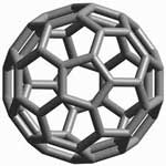
Life cycle assessment shows high energy requirements for fullerene production
There is a general perception that nanotechnologies will have a significant impact on developing 'green' and 'clean' technologies with considerable environmental benefits. However, the environmental footprint created by today's nanomanufacturing technologies are conflicting with the general perception that nanotechnology environmentally benign. It actually appears that certain nanomaterial production technologies are quite dirty and also have a considerable energy footprint. Determining the full environmental impact of nanomaterials requires a full life cycle assessment. A recent paper takes a look at the material and energy intensity of fullerene production. It finds that the embodied energy of all fullerenes are an order of magnitude higher than most common chemicals.
April 20, 2011
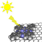
Novel hybrid graphene materials for solar cell applications
The extremely high electron mobility of graphene - under ideal conditions electrons move through it with roughly 100 times the mobility they have in silicon - combined with its superior strength and the fact that it is nearly transparent (2.3 % of light is absorbed; 97.7 % transmitted), make it an ideal candidate for photovoltaic applications. Recent research suggests, though, that doping is a necessity to harvest the full potential of graphene. The challenge then for researchers is to find suitable fabrication techniques for high-quality graphene flakes that exhibit high charge mobilities. Researchers now present a chemical approach towards non-covalently functionalized graphene, which is generated from vastly available and low-priced natural graphite.
April 19, 2011
Self-sintering conductive inks simplify printing of plastic electronics
Ink-jet printing of metal nanoparticles for conductive metal patterns has attracted great interest as an alternative to expensive fabrication techniques like vapor deposition. The bulk of the research in this area focuses on printing metal nanoparticle suspensions (metallic ink) for metallization. Printing conductive features by metallic nanoparticle inks must be followed by an additional step of sintering, usually achieved by heating to elevated temperatures. In this step, the nanoparticles composing the pattern will coalesce to form a continuous electrical contact. In new work, researchers have now demonstrated a new conductive ink that won't require a post printing sintering step. It is achieved by the addition of a latent sintering agent that gets into action after the printing step. Once the solvent evaporates, the sintering agent concentration increases, leading to the spontaneous sintering of the nanoparticles.
April 18, 2011

Why we don't need a regulatory definition for nanomaterials
Engineered nanomaterials present regulators with a conundrum - there is a gut feeling that these materials present a new regulatory challenge, yet the nature and resolution of this challenge remains elusive. But as the debate over the regulation of nanomaterials continues, there are worrying signs that discussions are being driven less by the science of how these materials might cause harm, and more by the politics of confusion and uncertainty. Yet the more we learn about how materials interact with biology, the less clear it becomes where the boundaries of this class of materials called "nanomaterials" lie, or even whether this is a legitimate class of material at all from a regulatory perspective.
April 15, 2011
Nanoporous quantum filters - inside the fascinating and weird world of confined quantum particles
One of the problems in modern separation science and technology is the challenge of separating gaseous mixtures that consist of very similar particles, for example, hydrogen isotope mixtures; mixtures of noble gases; etc. The problem arises because small particles such as hydrogen isotopes share similar size and shape (only their molecular mass is different). While this problem can be technically solved, currently available separation methods such as thermal diffusion, cryogenic distillation, and centrifugation, tend to be time and energy intensive. New theoretical work now shows that narrow carbon nanotubes (CNTs) seem to be an attractive alternative. By using CNTs as nanoporous molecular sieves, the separation of parahydrogen molecules from mixtures of classical particles at cryogenic temperatures seems to be possible.
April 14, 2011

Low-cost printing technique for a new generation of complex, flexible sensors
Printed electronics is one of the most important new enabling technologies. It will have a major impact on most business activities from publishing and security printing to healthcare, automotive, military and consumer packaged goods sectors. With recent advances, power and energy storage can be integrated into the printing process, making their potential applications even more ubiquitous. Currently, though, the more complex printed components that require a combination of different class of devices, still experience drawbacks in performance, cost, and large-scale manufacturability. Researchers have now succeeded in fabricating a multi-component sensor array by simple printing techniques - all components (polymer sensor array, organic transistors, electrochromic display) are integrated on the same flexible substrate.
April 13, 2011

Shooting videos in the nanoworld to observe nanoscale processes
Life as we know it is dominated by friction, the interaction between moving objects. Friction controls our everyday lives, from letting us walk to work, to holding a cup of tea. Friction forces act wherever two solids touch. Although friction has been investigated for hundreds of years - in the 15th century, Leonardo da Vinci was the first to enunciate two laws of friction - it is surprisingly difficult to examine how friction works at the nanoscale level due to the sheer difficulty of bringing nanoscale objects into contact and imaging them at the same time. Researchers have now demonstrated the ability to bring nanoscale objects together, rub them repeatedly across one another and see how friction changes nanosized materials in real time.
April 12, 2011

Does anyone know how much nanomaterials are produced? Anyone...?
Life cycle assessment is an essential tool for ensuring the safe, responsible, and sustainable commercialization of a new technology. With missing data about the large scale impact of nanotechnology, life cycle assessments of potential nanoproducts should form an integral part of nanotechnology research at early stages of decision making as it can help in the screening of different process alternatives. Part of any meaningful results from a life cycle assessment is the total quantity of the material under investigation. Especially exposure assessments often begin with estimates based on total amounts of a material produced with the assumption that some fraction of the material in question will ultimately released to the environment. As it turns out, nobody - no research institution, no government agency, no industry association - knows even vaguely how much nanomaterials are manufactured today.
April 11, 2011