What Is Nanotechnology? A Complete Beginner's Guide
Table of Contents
Key Takeaways About Nanotechnology
- Definition: Nanotechnology involves manipulating matter at the 1-100 nanometer scale to create materials and devices with novel properties
- Unique Properties: Nanomaterials exhibit different behaviors due to increased surface area and quantum effects not present in larger materials
- Applications: Currently used in medicine (including mRNA vaccines), electronics, energy, environmental remediation, agriculture, cosmetics, and manufacturing
- History: Term coined by Norio Taniguchi in 1974, though conceptualized by Richard Feynman in his 1959 talk
- Current Status: Nanotechnology is now mainstream, with leading-edge transistors at the 2 nm node and billions of lipid nanoparticle vaccine doses administered
- Manufacturing: Created through top-down (carving from larger materials) or bottom-up (self-assembly) approaches
- Future Potential: Developing areas include nanomedicine, quantum computing, energy storage, and nanobiotechnology
Understanding Nanotechnology: The Basics
What is Nanotechnology?
Nanotechnology is the science, engineering, and application of materials and devices designed at the nanoscale, which is roughly 1 to 100 nanometers. At this scale, increased surface area and quantum size effects give materials properties that are not seen in their bulk form, enabling novel uses across medicine, electronics, energy, and manufacturing.
A more formal definition describes nanotechnology as the imaging, modeling, measuring, design, characterization, production, and application of structures, devices, and systems by controlled manipulation of size and shape at the nanometer scale – that is, at the atomic, molecular, and macromolecular scale – producing structures, devices, and systems with at least one novel or superior characteristic or property (source).
The Nanoscale – How Small Is Nano?
Dimensions between approximately 1 and 100 nanometers are known as the nanoscale.
To see where 'nano' fits on the scale of things, check out our metric prefix table with examples and an interactive tutorial: View the Milky Way at 10 million light years from the Earth. Then move through space towards the Earth in successive orders of magnitude until you reach a tall oak tree. After that, begin to move from the actual size of a leaf into a microscopic world that reveals leaf cell walls, the cell nucleus, chromatin, DNA and finally, into the subatomic universe of electrons and protons.
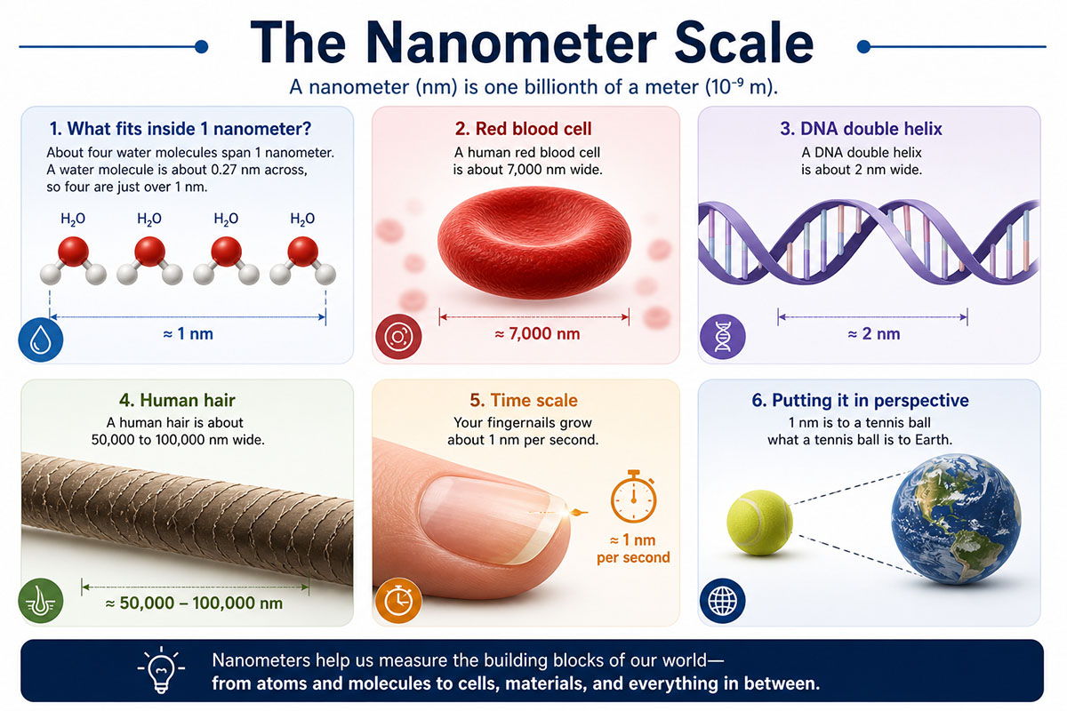
A nanometer is one billionth of a meter. (Image: Nanowerk) (click on image to enlarge)
Defining Nanotechnology (nan'o•tech•nol'o•gy) – It's Not That Simple...
One of the problems facing this technology is the confusion about how to define nanotechnology. Most revolve around the study and control of phenomena and materials at length scales below 100 nm and quite often they make a comparison with a human hair, which is about 50 000 to 100 000 nm wide.
For instance, in zero-dimensional (0D) nanomaterials all the dimensions are measured within the nanoscale (no dimensions are larger than 100 nm); in two-dimensional nanomaterials (2D), two dimensions are outside the nanoscale; and in three-dimensional nanomaterials (3D) are materials that are not confined to the nanoscale in any dimension. This class can contain bulk powders, dispersions of nanoparticles, bundles of nanowires, and nanotubes as well as multi-nanolayers. Check our Frequently Asked Questions to get more details.
Some definitions include a reference to molecular nanotechnology and 'purists' argue that any definition needs to include a reference to "functional systems".
Another important criteria for the definition is the requirement that the nanostructure is man-made, i.e. a synthetically produced nanoparticle or nanomaterial. Otherwise you would have to include every naturally formed biomolecule and material particle, in effect redefining much of chemistry and molecular biology as 'nanotech.
Who Coined the Term Nanotechnology?
The term was coined in 1974 by Norio Taniguchi of Tokyo Science University to describe semiconductor processes such as thin-film deposition that deal with control on the order of nanometers. His definition still stands as the basic statement today: "Nano-technology mainly consists of the processing of separation, consolidation, and deformation of materials by one atom or one molecule."
A second strand of meaning emerged in 1986, when American engineer K. Eric Drexler – apparently unaware of Taniguchi's earlier coinage – used the term in his book Engines of Creation: The Coming Era of Nanotechnology. Drexler used "nanotechnology" to describe a future based on programmable molecular "assemblers" that could build objects atom by atom, a vision now usually called molecular nanotechnology (MNT). The Drexlerian and the Taniguchi senses of the word have coexisted ever since: a near-term, top-down meaning rooted in precision manufacturing and a longer-term, bottom-up meaning rooted in molecular self-assembly. A famous 2003 exchange in Chemical & Engineering News between Drexler and Nobel laureate Richard Smalley publicly aired the disagreement over whether MNT-style assemblers were physically achievable, and the debate has continued in modified form to this day.
The everyday, policy-level meaning of "nanotechnology" was effectively settled in January 2000, when President Bill Clinton announced the U.S. National Nanotechnology Initiative (NNI) in a speech at Caltech. The NNI's working definition ("research and technology at the 1–100 nm scale that exhibits novel properties because of that scale") is the one that most government agencies, regulators, and standards bodies use today. Through fiscal year 2025, U.S. federal agencies have invested roughly $45 billion through the NNI, and similar national programs have followed in the EU, China, Japan, South Korea, and elsewhere.
Many argue that the conceptual history of nanotechnology starts even earlier, with Richard Feynman's classic talk in December 1959: There's Plenty of Room at the Bottom – An Invitation to Enter a New Field of Physics:
Why Nanotechnology Matters: Benefits and Impact
Why Does Nanotechnology Matter?
Unusual physical, chemical, and biological properties can emerge in materials at the nanoscale. These properties may differ in important ways from the properties of bulk materials and single atoms or molecules.
The bulk properties of materials often change dramatically with nano ingredients. Composites made from particles of nano-size ceramics or metals smaller than 100 nanometers can suddenly become much stronger than predicted by existing materials-science models.
For example, metals with a so-called grain size of around 10 nanometers are as much as seven times harder and tougher than their ordinary counterparts with grain sizes in the hundreds of nanometers. The causes of these drastic changes stem from the weird world of quantum physics. The bulk properties of any material are merely the average of all the quantum forces affecting all the atoms. As you make things smaller and smaller, you eventually reach a point where the averaging no longer works.
Surface Area and Quantum Size Effects
The properties of materials can be different at the nanoscale for two main reasons:
Surface Area
First, nanomaterials have a relatively larger surface area when compared to the same mass of material produced in a larger form. This can make materials more chemically reactive (in some cases materials that are inert in their larger form are reactive when produced in their nanoscale form), and affect their strength or electrical properties.
Quantum Size Effects
Second, quantum size effects can begin to dominate the behavior of matter at the nanoscale – particularly at the lower end – affecting the optical, electrical and magnetic behavior of materials. This effect describes the physics of electron properties in solids with great reductions in particle size. This effect does not come into play by going from macro to micro dimensions. However, it becomes dominant when the nanometer size range is reached.
We explain surface area and quantum size effects in detail in our explainer on why nanotechnology is so special.
The fascination with nanotechnology stems from these unique quantum and surface phenomena that matter exhibits at the nanoscale. They improve existing industrial processes, materials and applications in many fields – and allows entirely new ones.
How Nanomaterials Are Made and What They Do
How Nanomaterials Are Made: Top-Down and Bottom-Up
There are different ways of manipulating matter at the nanoscale. The two notions you hear most are top-down and bottom-up methods. Briefly, that means that you make a nanomaterial either by by taking a block of material and remove the bits and pieces you don't want until you get the shape and size you do want (that's top-down); or you use nature's self-organizing processes (that's called self-assembly) to build something from the bottom-up. The key to using self-assembly as a controlled and directed fabrication process lies in designing the components that are required to self-assemble into desired patterns and functions.
With regard to nanoscale materials, there are plenty of examples we could talk about here – nanoparticles, quantum dots, nanowires, nanofibers, ultrathin-films, MXenes, etc.
One example, though, that is exemplary of how an 'old' material gets an exciting new life through nanoscale technologies is the element carbon.
Natural carbon can exist in two very different types and is known to everyone: graphite and diamond. Three additional forms that were discovered between 1985 and 2004 have caused the current excitement among researchers about carbon nanomaterials – fullerenes, carbon nanotubes, and in particular graphene, often hyped as a 'wonder material'. Sumio Iijima's foundational work on carbon nanotubes was recognized with the inaugural 2008 Kavli Prize in Nanoscience, which he shared with Louis Brus for the discovery of semiconductor nanocrystals.
Current applications of nanomaterials include very thin coatings used, for example, in electronics and active surfaces (such as self-cleaning windows). In most applications the nanomaterial will be fixed or embedded but in some, such as those used in cosmetics and in some environmental remediation applications, free nanoparticles are used. The ability to engineer materials to very high precision and accuracy (smaller than 100nm) is leading to considerable benefits in a wide range of industrial sectors, for instance in the production of components for the information and communication technology, automotive and aerospace industries.
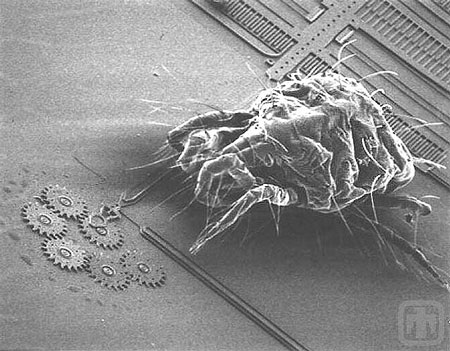
A mite, less than 1 mm in size, approaching a microscale gear chain. (Image: Sandia National Laboratories)
Some 20-30 years ago, microelectromechanical systems (MEMS) emerged in industrial manufacturing in a major way. MEMS consist of any combination of mechanical (levers, springs, membranes, etc.) and electrical (resistors, capacitors, inductors, etc.) components to work as sensors or actuators. The size of today's smartphones would be impossible without the use of numerous MEMS devices. Apart from accelerometers and gyroscopes, smartphones contain micro-mirrors, image sensors, auto-focus actuators, pressure sensors, magnetometers, microphones, proximity sensors and many more. Another example from everyday life is the use of MEMS as accelerometers in modern automobile airbags where they sense rapid deceleration and, if the force is beyond a programmed threshold, initiate the inflation of the airbag.
Then, researchers took a further step down the size scale and have begun exploring another level of miniaturization – nanoelectromechanical systems (NEMS). NEMS are showing great promise as highly sensitive detectors of mass, displacement, charge, and energy.
Nanoscience vs Nanotechnology – What's the Difference?
While closely related, nanoscience and nanotechnology have distinct focuses. Nanoscience is primarily concerned with understanding the fundamental properties and behaviors of materials at the nanoscale. In contrast, nanotechnology applies this knowledge to create materials, devices, and systems with unique functionalities for various applications. Essentially, nanoscience provides the foundation upon which nanotechnology is built.
Nanoscience And Nanotechnologies Are Not New
Chemists have been making polymers, which are large molecules made up of nanoscale subunits, for many decades, and the semiconductor industry has been etching and depositing features at the nanoscale on computer chips since the late 1990s.
However, advances in the tools that now allow individual atoms and molecules to be examined and probed with great precision have enabled the expansion and development of nanoscience and nanotechnologies. With new tools came new fundamental concepts and it turned out that the mechanical rules that govern the nanoworld are quite different from our everyday, macroworld experience.
In particular, ongoing quest for miniaturization has resulted in tools such as the atomic force microscope (AFM) or the scanning tunneling microscope (STM). Combined with refined processes such as electron beam lithography, these instruments allow the deliberate manipulation and manufacture of nanostructures. These instrument families are themselves still evolving: a 2025 study showed how machine learning can accelerate AFM analysis of cell mechanics, an example of how nanoscale tools and AI are now developing together.
Today there are a number of tools that can be used to characterize the nanomechanics of biomolecular and cellular interactions. Besides cantilever-based instruments like the AFM, examples include optical tweezers, and magnetic pullers.
What Does Nanotechnology Do?
Nanotechnology improves existing industrial processes, materials and applications by scaling them down to the nanoscale in order to ultimately fully exploit the unique quantum and surface phenomena that matter exhibits at the nanoscale. This trend is driven by companies' ongoing quest to improve existing products by creating smaller components and better performance materials, all at a lower cost.
This branch of engineering that deals with all aspects of the design, building, and use of engines, machines, and structures on the nanoscale is called nanoengineering (closely related to the terms nanofabrication and nanomanufacturing). At its core, nanotechnology engineering deals with nanoscale materials and how they interact to make useful materials, structures, and devices. It involves, nanostructuring, nanopatterning, and even 3D-printing (we explain nanoengineering in great detail here).
A prime nanotechnology example of an industry where nanoscale manufacturing technologies are employed on a large scale and throughout is the semiconductor industry where device structures have reached the single nanometers scale. Your smartphone, smartwatch or tablet all are containing billions of transistors on a computer chip the size of a finger nail.
So, what can nanotechnology do? There is almost no field today where nanotechnology isn't applied in some form or shape as things like surface coatings, sensors, electronic components, membranes, etc. – in medicine, environmental remediation, water filtration, nanoelectronics, food and agriculture, cosmetics, energy and batteries, space and aeronautics, automotive industries, displays, sports equipment and many more.
Our Learning Hub has in-depth articles on all of these topics.
Many products are defined as "nanotechnology product" because they contain nanoparticles in some form or other. For instance, many antimicrobial coatings contain silver in nanoscale form; food products and cosmetics contain nanoparticles; and some products are partially made with composite materials containing nanomaterials (e.g. carbon nanotubes or -fibers) to mechanically strengthen the material.
More advanced fields of nanotechnology deal with nanobiotechnology (the application of nanotechnologies in biological fields) and nanorobotics – not to be confused with the fictional nanorobots in science fiction.
Real-World Applications of Nanotechnology by Industry
Electronics and Information Technology
Nanotechnology has a profound impact on the electronics industry, particularly in semiconductors for computing devices. The miniaturization of transistors, the building blocks of any electronic device, has been driven by nanotechnology. Leading foundries such as TSMC, Samsung, and Intel are now producing chips at the 2 nm node, with 3 nm widely deployed across high-volume devices and development progressing toward even smaller scales. Your smartphone contains billions of transistors on a chip the size of a fingernail, with individual transistors now smaller than a virus.
Another significant development is quantum dots—semiconductor nanocrystals typically 2-10 nanometers in diameter. Their size-dependent optical properties (smaller dots emit blue light, larger dots emit red) have made them valuable for display technology. Samsung's QLED televisions use quantum dots to achieve enhanced color accuracy and brightness, and the research frontier has now moved to flexible quantum-dot displays with ultra-high resolution and bending stability. The importance of this technology was recognized when Moungi Bawendi, Louis Brus, and Alexei Ekimov received the 2023 Nobel Prize in Chemistry for their discovery and development of quantum dots.
Furthermore, novel concepts such as spintronics and memristors are also being explored thanks to nanotechnology. Spintronics uses the spin of electrons, in addition to their charge, to carry information – potentially enabling computers that are faster and more energy efficient. Memristors are circuit elements whose resistance depends on the history of current that has flowed through them – a property useful for non-volatile memory, digital logic, and neuromorphic computing.
Nanotechnology has also enabled the development of MEMS (Micro-Electro-Mechanical Systems) and NEMS (Nano-Electro-Mechanical Systems) which are employed in a wide array of sensors and actuators in various devices such as smartphones, wearable devices, and automobile airbag systems.
Medicine and Healthcare
The most visible demonstration of nanotechnology's medical impact came during the COVID-19 pandemic. The mRNA vaccines from Pfizer-BioNTech and Moderna use lipid nanoparticles (LNPs)—tiny fat bubbles approximately 80-100 nanometers in diameter—to deliver fragile genetic instructions into human cells. Billions of doses have been administered worldwide, demonstrating that nanomedicine can work safely at massive scale. This technology is now being applied to develop vaccines for other diseases and to deliver mRNA therapeutics for conditions ranging from cancer to genetic disorders.
Beyond vaccines, nanomedicine encompasses targeted drug delivery systems that send medicine directly to diseased cells, reducing side effects and improving the efficacy of treatment. FDA-approved nanomedicines like Doxil (liposomal doxorubicin) and Abraxane (albumin-bound paclitaxel) use nanoparticle formulations to improve cancer treatment. Additionally, nanoparticles are being used in imaging for improved diagnostics and surgical precision.
Energy Generation and Storage
In the energy sector, nanotechnology is driving significant advances in both energy generation and storage. In solar energy, perovskite solar cells represent the most exciting development in photovoltaics in decades. These cells use nanostructured perovskite crystals that can be manufactured at low temperatures. Single-junction perovskite cells have reached 26.7% efficiency, while perovskite-silicon tandem cells have achieved 34.6%—approaching theoretical limits that conventional silicon alone cannot reach.
In energy storage, nanostructured materials are revolutionizing batteries for electric vehicles. Silicon can theoretically store ten times more lithium than conventional graphite anodes, but it swells dramatically during charging. Nanostructured silicon—using nanowires, nanoparticles, or nanoporous structures—accommodates this expansion. Companies are now commercializing silicon anode batteries with significantly higher energy density and faster charging times. Nanotechnology also enables more effective fuel catalysts and improved hydrogen storage materials for fuel cells.
Environmental Remediation
Nanotechnology is also being applied to environmental remediation. Nanoparticles can be engineered to clean up industrial contamination, making polluted water safe to drink or polluted air safe to breathe. Additionally, nanotechnology can contribute to improved filtration and purification processes, aiding in the removal of contaminants from water supplies.
A particularly active area is the removal of per- and polyfluoroalkyl substances (PFAS), the "forever chemicals" whose long C–F bonds resist conventional water treatment. Nanomaterial-enhanced membranes, graphene-nanoplatelet adsorbents, and metal-organic frameworks (MOFs) have all reached the lab- and pilot-scale demonstration stage between 2023 and 2026, with several reports of trace-level PFAS removal at >99% efficiency. The U.S. EPA's first enforceable national drinking-water limits for PFOA and PFOS, finalized in April 2024 at 4 parts per trillion (with parallel regulatory activity on additional PFAS still ongoing), have sharpened the demand for cost-effective treatment, and nanotechnology is one of the leading candidate technology families being evaluated by water utilities.
Beyond PFAS, nanoscale zero-valent iron is now used in groundwater remediation for chlorinated solvents at multiple sites, and nanostructured photocatalysts based on titanium dioxide and bismuth-based materials are being deployed for indoor air cleaning and self-cleaning surfaces.
Agriculture
Nanotechnology's applications in agriculture aim to increase productivity and protect crops, all while minimizing potential environmental impacts. For instance, nanosensors are being utilized to monitor soil quality and detect diseases or pests, enabling timely and localized application of treatment. Furthermore, nano-encapsulation of fertilizers and pesticides improves the efficiency of nutrient and pest management, reducing the overall quantity of these substances needed, and mitigating their runoff into surrounding ecosystems. Nano-fabricated "smart" delivery systems can precisely release nutrients or medicines in response to environmental triggers, leading to improved plant health and yield.
The most concrete example of large-scale agricultural nanotechnology to date is India's nano urea program. The Indian Farmers Fertiliser Cooperative (IFFCO) launched commercial liquid nano urea in 2021 and nano DAP in 2023; by 2024–2025 seven nano urea plants were in operation with a combined capacity of more than 270 million 500 ml bottles per year, and India had begun exporting nano urea to Bangladesh, Brazil, Kenya, and Vietnam. In March 2026 the Indian government brought 14 nano-fertiliser products formally into the regulatory fold under the Fertiliser Control Order, with a specification that at least 50% of particles must be below 100 nm. Independent field studies have produced mixed results on yield, however, and adoption rates among farmers vary widely – a useful reminder that "commercially deployed" and "agronomically settled" are different things.
Cosmetics
In the cosmetics industry, nanotechnology is used to enhance the properties and effectiveness of products. Nanoparticles, due to their small size, can penetrate deeper layers of the skin, improving the delivery of active ingredients. For example, nanoparticles of zinc oxide or titanium dioxide are used in sunscreens for better protection against harmful UV rays, while maintaining transparency to avoid a white residue on the skin. Also, nanoemulsions are used to improve the texture and feel of products, and for controlled release of fragrances or active ingredients.
Cosmetics is also where the regulatory environment around engineered nanomaterials has shifted most visibly. In March 2024 the European Commission published Regulation (EU) 2024/858, banning twelve nanomaterials – including nano styrene/acrylates copolymer and several colloidal gold and platinum forms – from cosmetic products, with non-compliant products having to be withdrawn from sale by November 2025. Titanium dioxide remains under active reassessment: the Scientific Committee on Consumer Safety (SCCS) concluded in May 2024 that the available evidence is insufficient to exclude the genotoxicity of most nano- and pigmentary TiO2 grades used in oral cosmetic products such as toothpastes and lipsticks, while a separate June 2025 EU court ruling overturned the broader carcinogen classification of titanium dioxide for industrial CLP purposes. The combined effect is that "nanomaterial" is now a defined and labelled regulatory category in EU cosmetics, not a marketing buzzword.
Food and Packaging
Nanotechnology finds its application in the food industry as well, primarily aimed at improving food safety, quality, shelf life, and nutritional content. For instance, nano-encapsulated food additives or nutrients can enhance flavor and nutritional value, or provide controlled release to improve shelf life. Nanosensors are being used for real-time monitoring of food quality and safety, detecting microbial contamination, and monitoring storage conditions. Nanotechnology can also be used to create 'smart' packaging materials with improved barrier properties, antimicrobial activity, or indicators for freshness or contamination.
Nanocellulose – cellulose nanocrystals (CNCs) and cellulose nanofibers (CNFs) extracted from wood pulp, agricultural residues, or bacterial sources – has emerged as one of the most active areas of food-packaging nanotechnology, with multiple producers now operating at industrial scale across Europe, North America, and Asia. CNF-reinforced biodegradable films can lower oxygen and water-vapor permeability by an order of magnitude relative to baseline bio-polymers, addressing the main shortcoming that has historically held compostable packaging back. The packaging segment of the cellulose nanocrystals and nanofibers market was valued in the hundreds of millions of dollars in 2024 and is forecast to grow at roughly 20% per year through the early 2030s.
Materials and Manufacturing
Nanotechnology has facilitated the development of materials with enhanced properties, such as improved strength, lightness, durability, and responsiveness to environmental cues. For instance, many products are partially made with composite materials containing nanomaterials to mechanically strengthen the material. In manufacturing, nanotechnology allows for precise, atomic-level control over material structures, leading to innovations in a wide range of industrial sectors, including automotive, aerospace, and consumer products.
A high-impact recent example is graphene-enhanced concrete. Cement production accounts for roughly 8% of global CO2 emissions, and adding small fractions (typically below 0.1% by weight) of graphene oxide or graphene nanoplatelets to the mix has been shown to improve compressive strength, reduce porosity, and allow 20–30% less cement to be used for the same structural performance. UK-based Concretene completed its first real-world pour at a gym in Amesbury in 2021, was incorporated as a separate company in 2022 with backing from Arup, and ran further field trials with precast concrete partners and Cemex through 2024 and 2025. Spain's Graphenano Smart Materials reports having sold more than 1,000 tonnes of its graphene additive to ready-mix and precast concrete producers, and several other companies are now competing in the same space – the first concrete commercial deployments of a long-promised graphene application.
Finally, A Word Of Caution
Truly revolutionary nanotechnology products, materials and applications, such as nanorobotics, are years in the future (some say only a few years; some say many years). What qualifies as "nanotechnology" today is basic research and development that is happening in laboratories all over the world.
"Nanotech" products that are on the market today are mostly gradually improved products (using evolutionary nanotechnology) where some form of nano-enabled material (such as carbon nanotubes, graphene, nanocomposite structures or nanoparticles of a particular substance) or nanotech process (e.g. nanopatterning or quantum dots for medical imaging) is used in the manufacturing process.
There are also environmental, health and safety considerations associated with nanotechnology and nanomaterials. However, comprehensive regulatory frameworks now govern nanomaterials in major markets, and the safe administration of billions of mRNA vaccine doses demonstrates that nanomaterials can be used safely when properly designed and tested. We discuss nanotechnology safety and regulation in detail here.
Frequently Asked Questions (FAQ) on Nanotechnology
What is nanotechnology?
Nanotechnology is the science, engineering, and application of materials and devices with structures, properties, and performance characteristics designed at the nanoscale, which is about 1 to 100 nanometers.
What are the benefits of nanotechnology?
Nanotechnology can lead to major advancements in various fields. It can result in more efficient energy sources, enable advanced medical treatments, produce stronger and lighter materials, and much more.
Are there any risks associated with nanotechnology?
Like any technology, nanotechnology has potential risks that must be managed. The field of nanotoxicology studies potential effects, and safe-by-design approaches integrate safety considerations from the earliest stages of development.
How is nanotechnology regulated?
In the European Union, nanomaterials are regulated under REACH (Registration, Evaluation, Authorisation and Restriction of Chemicals), requiring companies to submit dedicated registration dossiers to the European Chemicals Agency (ECHA). In the United States, the EPA regulates nanomaterials under the Toxic Substances Control Act (TSCA), with specific reporting requirements for nanoscale materials. Additional sector-specific regulations cover nanomaterials in cosmetics, food, biocides, and medical devices. The OECD Working Party on Manufactured Nanomaterials coordinates international testing guidelines.
Who are the leading players in nanotechnology?
These are too numerous to list. There are many companies and academic institutions across the globe leading the way in nanotechnology, including semiconductor manufacturers like TSMC, Samsung, and Intel; pharmaceutical companies developing nanomedicines; and thousands of specialized nanotechnology companies. Check out our Companies & Laboratories database for more.
What is a nanobot?
A nanobot (or nanorobot) is a tiny machine designed at the nanoscale. It's a theoretical concept at present, with potential applications in medicine and manufacturing.
What are nanomaterials?
Nanomaterials are materials that have at least one dimension (height, width, or length) that is less than 100 nanometers. They have unique properties compared to their larger counterparts.
What's the difference between nanoscience and nanotechnology?
Nanoscience is the study of phenomena and manipulation of materials at the nanoscale, while nanotechnology applies the findings of nanoscience to create devices or structures at the nanoscale.
