| Posted: Mar 28, 2007 |
Label-free nanobiosensing platforms |
| (Nanowerk Spotlight) People involved in designing and developing biosensing applications have high hopes that their field can benefit from nanotechnology. The term biosensing relates to systems that include electronic, photonic, biologic, chemical and mechanical means for producing signals that can be used for the identification, monitoring or control of biological phenomena. The resulting biosensors are devices that employ biological components such as proteins to provide selectivity and/or amplification for the detection of biochemical materials for use in medical diagnostics, environmental analysis or chemical and biological warfare agent detection. Applying nanotechnology to biosensors opens up novel detection possibilities thanks to the nano-physical properties of certain materials. A lot of research worldwide is devoted to developing nanobiosensors. A group in Switzerland, for example, is working on the development of two different kinds of label-free biosensors. One is a nanowire array, the other an optical biosensor based on localized surface plasmon resonance. |
| The two core functionalities of a biosensor are selectivity (to measure the desired substance or substances) and sensitivity (how low a quantity of the measured substance can be detected). Selectivity requires the relevant biomolecular recognition elements such as antibodies or enzymes to be fixed on a receptor membrane. For highest sensitivity, great efforts have been made to get access to single surface-immobilized biomolecules. Single protein nanoarrays have the advantage over homogeneous or micropatterned surfaces that the interaction between single biomolecules, rather than an average signal, can be monitored. |
| There are various approaches to creating nanotemplates; among them are top-down approaches, mainly lithography-based techniques, or bottom-up methods, such as colloidal lithography, which take advantage of self-assembly. In addition, the self-assembly capability of biomolecules has turned out to be very helpful in selectively decorating/activating surfaces in the nanorange. In particular DNA should be noted as a useful construction tool for engineering nanodevices via self-assembly. |
| "We developed a platform which enables the precise positioning of DNA-tagged gold colloids onto single dot and line arrays and has the potential to serve as a label-free biosensing platform" Dr. Janos Vörös explains to Nanowerk. "Our approach is unique in that we can produce a great number of large-scale periodic nanopatterns without drastic limitations of the substrate, the linkage chemistry or of the detection method." |
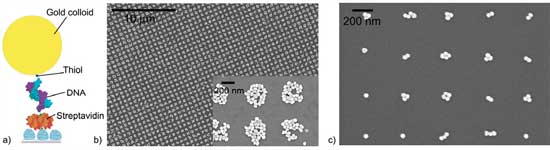 |
(a) Complexes of neutravidin and single-stranded biotinylated DNA were added to the biotinylated spots via the biotin/avidin linkage. 50 nm gold colloids tagged with the complementary DNA via a thiol bond could specifically hybridize to the surface, as shown on the SEM image, on (b) 270 nm dots and (c) 100 nm dots. (Reprinted with permission from IOP Publishing) |
| Vörös is a professor at the Swiss Federal Institute of Technology Zurich where he heads the Laboratory of Biosensors and Bioelectronics. Together with a group of collaborators his lab developed a fabrication process that separates the nanolithography step from the functionalization step. |
| This process is based on extreme ultraviolet interference lithography (EUVIL) which creates substrates with photoresist patterns in the nanorange. These surfaces are transformed into arrays of gold colloids. A biotin–avidin linkage is then used to surface-immobilize complexes of streptavidin and single- stranded DNAs, which then offered the anchoring points for the nano-objects tagged with the complementary DNA. |
| "The separation between the lithography and the subsequent functionalization of the nanoarray has many advantages," says Vörös. "1) The biotin–streptavidin system used can be replaced by other linkage chemistries such as nitrilotriacetic acid–histidin or mannose–lectin. 2) The gold colloids can be functionalized and used for example for basic cell–surface interaction studies. 3) This patterning approach can readily be applied to other nano-objects, such as vesicles or proteins, that can be tagged with DNA. 4) The concept has a potential for mass production because the created patterns could be transferred to another substrate by ‘stamping’." |
| The approach taken by the Swiss researchers is unique in the sense that it can be applied from micron sizes down to the sub-100 nm range. The resulting nanopatterns are covering quite a large area – a few square millimeters. |
| This work could lead to two kinds of label-free biosensors: A nanowire-based device which might detect the binding of biomolecules via a change in conductivity; and an optical biosensor based on the change of exited plasmons upon adsorption of biomolecules to the noble metal colloids. The later is based on the fact that in noble metal colloids plasmons can be excited at a specific wavelength. This wavelength depends on many factors among them the dielectric constant of the environment. |
| Vörös points out that is has been shown that this way the adsorption of biomolecules to noble metal colloids can be detected but still there are many open questions – e.g. the coupling between the neighboring colloids can not be properly accounted for. "We are addressing this issue by producing arrays with a controlled number of gold colloids to compare computational models with experiments" he says. |
| Vörös and his collaborators reported their findings, titled "Nanopatterning of gold colloids for label-free biosensing", in the March 9, 2007 online issue of Nanotechnology. |
 By
Michael
Berger
– Michael is author of four books by the Royal Society of Chemistry:
Nano-Society: Pushing the Boundaries of Technology (2009),
Nanotechnology: The Future is Tiny (2016),
Nanoengineering: The Skills and Tools Making Technology Invisible (2019), and
Waste not! How Nanotechnologies Can Increase Efficiencies Throughout Society (2025)
Copyright ©
Nanowerk LLC
By
Michael
Berger
– Michael is author of four books by the Royal Society of Chemistry:
Nano-Society: Pushing the Boundaries of Technology (2009),
Nanotechnology: The Future is Tiny (2016),
Nanoengineering: The Skills and Tools Making Technology Invisible (2019), and
Waste not! How Nanotechnologies Can Increase Efficiencies Throughout Society (2025)
Copyright ©
Nanowerk LLC
|

Become a Spotlight guest author! Join our large and growing group of guest contributors. Have you just published a scientific paper or have other exciting developments to share with the nanotechnology community? Here is how to publish on nanowerk.com.
