| Posted: Sep 05, 2012 |
Highly asymmetric line nanopatterning becomes possible with block copolymer self-assembly |
| (Nanowerk Spotlight) Lithography based on block copolymer self-assembly has received significant attention due to the ability to achieve morphologies with dimensions in the range of 10 to 20 nm or even below. Block copolymer lithography is a cost-effective, parallel, and scalable nanolithography for densely packed periodic arrays of nanoscale features, whose typical dimension scale is beyond the resolution limit of conventional photolithography (see our Nanowerk Spotlight: "Novel nanoimprint technique offers a low-cost route toward sub-10 nm nanopatterning"). |
| Typically, the block copolymer microdomains used for this purpose are periodic lamellar microdomains. Such lamellar microdomains usually arise only in a narrow range of block compositions in which the volume fractions of the two components are approximately the same. |
| "For next-generation line patterns required for nanolithography, the technology needs to be extended to obtain highly asymmetric line patterns at the nanoscale, similar to those that could be obtained by top-down approach such as e-beam lithography – which is a slow and extremely expensive process," Jin Kon Kim a professor in the Department of Chemical Engineering at Pohang University of Science and Technology, and Director of National Creativity Research Initiative Program for Block Copolymer Self Assembly, explains to Nanowerk. "Hence, we prepared highly asymmetric lamellar microdomains by the use of binary blends of block copolymers whose components are capable of H-bonding, and also demonstrated thin-films with asymmetric lamellar line patterns oriented vertically on a silicon wafer." |
| In new work, reported in the August 20, 2012 online edition of ACS Nano ("Highly Asymmetric Lamellar Nanopatterns via Block Copolymer Blends Capable of Hydrogen Bonding"), Kim and his team introduce a conceptually new and versatile strategy to achieve asymmetric line patterns. This is the first work to demonstrate that highly asymmetric line nanopatterning is possible even though a block copolymer self-assembly technique is used. |
| "It is known that when the volume fraction of one block is quite different from the other block, lamellar – or line – patterning is impossible due to the formation of more stable nanostructures of cylindrical or spherical shapes," says Kim. "We solved this problem by introducing hydrogen bonding between the blocks which changes from curvature nanostructures to line – or lamellar – nanopatterns." |
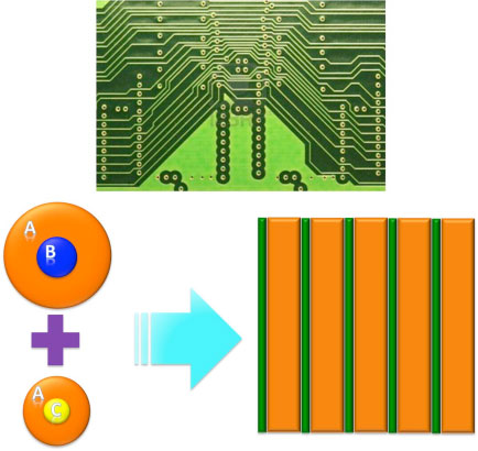 |
| Top: Circuit line patterns with various line widths in a computer RAM memory. Bottom: Schematic of the fabrication of asymmetric line patterning by using hydrogen (H-) bonding. Bottom left: Two neat block copolymers (A-B and A-C) with highly asymmetric composition copolymers. Both show curved nanodomains (spherical nanodomains), not flat (or line) nanodomains (or lamellae). However, when H-bonding is formed between B and C chains by mixing A-B and A-C, the spherical nanodomains become lamellar nanodomains with highly asymmetric line widths. (Image: Dr. Kim, Pohang University of Science and Technology) |
| Through theoretical and experimental results they show that the H-bonding interaction between the blocks plays a crucial role in fabricating asymmetric lamellar microdomains (or nanodomains) and can be used as a strategy to fabricate tunable asymmetric lamellar morphologies with sub-10 nm sizes required for nanolithographic applications. |
| In this study, the etching contrast between two blocks has not been large enough for the application of block copolymer thin-films to fabricate lithographic pattern transfer. The researchers note, however, that the etching contrast between polystyrene (PS) and poly(2-vinyl pyridine) (P2VP) (or poly(4-hydroxy styrene) (PHS)) can be easily enhanced by over-staining of the P2VP (or PHS) block using iodine due to the higher staining power of P2VP (or PHS) to iodine. Theoretical calculations indicate that asymmetric line patterns are achievable over a wide range of interaction parameters between blocks. |
| Kim points out that these results could be directly applied to next-generation lithography where sub-10 nm width as well as asymmetric lamellar nanopatterns is obtained, which cannot be achieved using symmetric block copolymers. |
| "Moreover" he says, "since the asymmetry in the microdomain sizes is mainly determined by the ratio of the volume fraction of the A (PS) component relative to the B (P2VP) and C (PHS) components in our blend, our approach provides easy and versatile control of the asymmetry of the line widths in a large area." |
| In summary, this novel strategy using binary blends of block copolymer capable of H-bonding enables the preparation of various nanopatterns – something that is impossible with conventional block copolymer. Furthermore, if the vertical orientation of asymmetric lamellae can be achieved for thin-films of a binary blend of polymethylmethacrylate (PMMA)-b-P2VP and PMMA-b-PHS, lithographic pattern transfer could be facilitated because the PMMA block can be selectively removed by UV irradiation and rinsing with acetic acid. |
 By
Michael
Berger
– Michael is author of four books by the Royal Society of Chemistry:
Nano-Society: Pushing the Boundaries of Technology (2009),
Nanotechnology: The Future is Tiny (2016),
Nanoengineering: The Skills and Tools Making Technology Invisible (2019), and
Waste not! How Nanotechnologies Can Increase Efficiencies Throughout Society (2025)
Copyright ©
Nanowerk LLC
By
Michael
Berger
– Michael is author of four books by the Royal Society of Chemistry:
Nano-Society: Pushing the Boundaries of Technology (2009),
Nanotechnology: The Future is Tiny (2016),
Nanoengineering: The Skills and Tools Making Technology Invisible (2019), and
Waste not! How Nanotechnologies Can Increase Efficiencies Throughout Society (2025)
Copyright ©
Nanowerk LLC
|

Become a Spotlight guest author! Join our large and growing group of guest contributors. Have you just published a scientific paper or have other exciting developments to share with the nanotechnology community? Here is how to publish on nanowerk.com. |
