| Posted: Apr 15, 2008 |
Conductive and tunable transparent coatings made from monodisperse carbon nanotubes |
| (Nanowerk Spotlight) There are several touch sensor technologies available to power touch screens like the ones you can find on your bank ATM, airport check-in kiosk or other self-service terminals. What they all have in common is that they are sensitive to human touch because their screens are coated with a special transparent thin film that act as a sensor. This sensor generally has an electrical current or signal going through it and touching the screen causes a voltage or signal change. Apart from touch screens, transparent conductive thin films are used in numerous products such as flat-panel displays, solar cells or as thermal barriers in energy-saving windows. Future applications will include flexible displays for e-papers, smart cards, 'heads-up' displays integrated into cockpit and car windows, and windows that can be used as a light source at night. |
| The technology to manufacture transparent, electrically conductive layers on transparent substrates is highly developed but suffers from reliance on the most widely used standard material - indium tin oxide (ITO). There are several problems with ITO that make it less than optimal for these applications: It is relatively brittle, which degrades its performance on flexible substrates; it has limited chemical stability leading to corrosion in device structures; its electrical properties greatly depend on the film preparation; and, most importantly, the Earth is running out of indium, making this material more and more expensive. |
| All this has driven increased research activity in finding alternative novel transparent electrode materials with good stability, high transparency and excellent conductivity. Graphene is one good candidate (see: Ultrathin transparent graphene films as alternative to metal oxide electrodes) and films based on carbon nanotubes have attracted significant attention recently as well. Researchers now have demonstrated the use of metallic nanotubes to make thin films that are semitransparent, highly conductive, flexible and come in a variety of colors. |
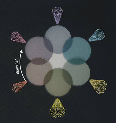 |
| Photograph of conductive, flexible carbon nanotube 'stained glass' on flexible plastic substrates. The carbon nanotube films are arranged in order of increasing average diameter (clockwise starting from lower left): 0.9, 1.0, 1.05, 1.1, 1.4, and 1.6 nanometers. The ability to control nanotube diameter leads to the visible colors that are apparent in the photograph. (Image: Dr. Mark Hersam) |
| "While there has been much progress in the development of single-walled carbon nanotube (SWCNT) transparent conductors in recent years, previous work has been limited by the unavoidable polydispersity of as-produced SWCNTs" Dr. Mark C. Hersam, a professor of Materials Science and Engineering at Northwestern University in Evanston, Illinois, explains to Nanowerk. "This polydispersity stems from the unique structure of SWCNTs. Although this structure imbues them with their remarkable characteristics, it also renders their properties highly sensitive to the nanotube diameter and helicity. Of all possible SWCNT chiralities, roughly one-third are metallic with the remainder being semiconductors whose bandgaps vary inversely with nanotube diameter." |
| This polydispersity problem – where a given batch of SWCNTs contains material with a distribution of diameters and varying electronic character – also caused less than optimal results in previous work on transparent conductive nanotube networks because of the broad distribution of electrical and optical characteristics of the involved nanotube material. |
| Utilizing a technique known as density gradient ultracentrifugation (DGU), Hersam's group has produced SWCNTs with uniform electrical and optical properties, enabling the production of transparent conductors consisting predominantly of metallic SWCNTs with small diameter distributions. Thin films formulated from these high purity carbon nanotubes possess 10-fold improvements in conductivity compared to pre-existing carbon nanotube materials. |
| Hersam explains that in the DGU process SWCNTs undergo ultracentrifugation, after which colored bands of sorted SWCNTs can be recovered and incorporated directly into transparent conductive films. |
| "Films generated from sorted metallic SWCNTs offer two major improvements over those produced from unsorted material" he says. "First, DGU eliminates poorly conducting, strongly absorbing carbonaceous impurities and semiconducting SWCNTs to enhance transparent conductor electrical performance and optical transmissivity. Second, since the optical absorption of metallic SWCNTs is strongly dependent on diameter, the angstrom-level control over nanotube diameter afforded by DGU results in films possessing a variety of different colors. These semitransparent conductive SWCNT coatings offer an unprecedented degree of control over the optical properties of the transparent conductor." |
| SWCNTs sorted this way can be tuned with much higher fidelity than ITO, which can only be controlled in a much coarser way through film thickness and doping level. It is expected that metallic SWCNTs of monodisperse diameter will increasingly challenge ITO in transparent conductor applications, particularly those in which a high degree of optical tunability is required. |
| "We expect conductive SWCNT coatings to enhance transparent conductor performance in multiple applications" says Hersam. "High transmittance regions of optimized films could be employed to increase the efficiency of devices such as flat panel displays, light emitting diodes, and solar cells. Conversely, the sharply peaked low transmittance regions of the coatings could be used to filter out unwanted portions of the optical spectrum that compromise device performance." |
| He points out that high-purity carbon nanotube thin films not only have the potential to make inroads into current applications but also accelerate the development of emerging technologies such as organic light-emitting diodes and organic photovoltaic devices. "These energy-efficient and alternative energy technologies are expected to be of increasing importance in the foreseeable future." |
| Hersam and first author Alexander Green, a graduate student in Hersam's group, have published their findings in the April 8, 2008 online edition of Nano Letters ("Colored Semitransparent Conductive Coatings Consisting of Monodisperse Metallic Single-Walled Carbon Nanotubes"). |
 By
Michael
Berger
– Michael is author of four books by the Royal Society of Chemistry:
Nano-Society: Pushing the Boundaries of Technology (2009),
Nanotechnology: The Future is Tiny (2016),
Nanoengineering: The Skills and Tools Making Technology Invisible (2019), and
Waste not! How Nanotechnologies Can Increase Efficiencies Throughout Society (2025)
Copyright ©
Nanowerk LLC
By
Michael
Berger
– Michael is author of four books by the Royal Society of Chemistry:
Nano-Society: Pushing the Boundaries of Technology (2009),
Nanotechnology: The Future is Tiny (2016),
Nanoengineering: The Skills and Tools Making Technology Invisible (2019), and
Waste not! How Nanotechnologies Can Increase Efficiencies Throughout Society (2025)
Copyright ©
Nanowerk LLC
|

Become a Spotlight guest author! Join our large and growing group of guest contributors. Have you just published a scientific paper or have other exciting developments to share with the nanotechnology community? Here is how to publish on nanowerk.com.
