| Posted: Jul 03, 2007 | |
Nanotechnology fabrication depends on sophisticated simulation tools |
|
| (Nanowerk Spotlight) Continuing miniaturization has moved the semiconductor industry into the nano realm with leading chip manufacturers well on their way to CPUs using 32nm process technology (expected by 2009). | |
| There are some real challenges ahead for chip designers, particularly in moving deeper and deeper into the nanoscale, where at some point in the near future they will reach physical limits of the traditional logic MOSFET (metal-oxide-semiconductor field-effect transistor) structure. | |
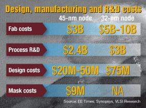
| In addition to physical barriers, semiconductor companies will also reach economic barriers where profitability will be squeezed hard in view of the exorbitant costs of building the necessary manufacturing capabilities if present day technologies are extrapolated. | |
| Quantum and coherence effects, high electric fields creating avalanche dielectric breakdowns, heat dissipation problems in closely packed structures and the relevance of single atom defects are all roadblocks along the current road of miniaturization. Enter nanoelectronics (note that microelectronics, even if the gate size of the transistor is below 100 nm, is not an implementation of nanoelectronics, as no new qualitative physical property related to reduction in size are being exploited). | |
| Its goal is to process, transmit and store information by taking advantage of properties of matter that are distinctly different from macroscopic properties. Understanding nanoscale transport and being able to model and simulate nanodevices requires an entirely new generation of simulation tools and techniques. | |
| Nanoelectronics has the potential to displace large parts, if not all, of conventional semiconductor applications. Transistors and silicon could become a relict as scientists are looking at all kinds of new ways of building nanoscale information processing devices based on quantum computing; modeled after living systems; DNA-based; or some form of silicon-biological hybrid. Even the term "electronics" might be doomed as it is far from clear that electrons will be the method of choice for signal processing or computation in the long term (take a look at our recent Nanowerk Spotlight "The road to molecular computing"). | |
| For the foreseeable future, though, semiconductor manufacturing is alive and kicking, and advances in nanoelectronics are slow and still very basic. Before we see an IBM 'Wet Blue' or some other form of non-silicon computer, traditional design and fabrication paradigms still hold. Nevertheless, increasing research in the field of nanoelectronics also requires the rise of a new generation of supporting fields, such as modeling and simulation tools. | |
| Semiconductor manufacturing is an extreme example for a technology where prototyping next generation devices is always very demanding, especially from an economic point of view. As the cost for each new generation of chips rises to staggering heights, there is no room for error and modeling an simulation is an important factor during the design stage. | |
 |
|
| This is why engineers and designers rely on software tools to simulate new devices without physically building them. Once the software computes and shows all the desired characteristics of a simulated device, then engineers are able to build a prototype, minimizing – and ideally eliminating – the risk of failure. | |
| Traditional transport models for semiconductor devices treat electrons and holes as classical particles or a classical carrier gas. A vast software resource exists for the modeling of semiconductor devices using such classical approaches. However, as the device lengths decrease down to the nanometer scale, the boundaries between device and material become blurry. Quantum mechanical effects of the underlying material structure dominate device characteristics. | |
| "Among the various simulation techniques, the most advanced is certainly the so-called Monte Carlo simulation method, based on the solution of particles physics and transport by means of random numbers" Dr Jean Michel Sellier explains to Nanowerk. "Even if it sounds quite eccentric to simulate the deterministic behavior of particles in a device by means of random numbers, this method has already been utilized successfully for the simulation of micron and sub-micron devices and has been recently modified in order to simulate nanoscale devices where the quantum effects start to become an issue." | |
| Sellier is the founder of SouthNovel, a semiconductor software company that developed Aeneas3, a very advanced simulator for Monte Carlo quantum transport in semiconductor devices of general 3D shape for organic and inorganic materials. | |
| Some nanodevices already have been successfully simulated, showing the interesting features of the nanoelectronics to come. With Aeneas it is now possible to simulate Monte Carlo particles transport in devices of nanoscale dimensions, taking into account not only all the relevant quantum effects, but also very general shapes. | |
  |
|
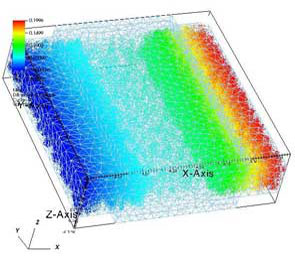
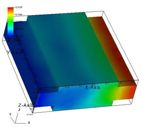
| These images represent the simulation of a double gate MOSFET, a particular kind of nanodevice which will soon substitute the traditional MOSFETs. Left: electrons in the mesh of the device. The color represents the potential these electrons are experiencing during the simulation. Right: The calculated potential of the device through Aeneas. (Images: SouthNovel) | |
| "In fact, one of the very important and advanced characteristic of new electronic device structures is that they can be completely 3D and of various shapes – very different from those in microelectronics" says Sellier. "Until now, software able to simulate completely general 3D shapes was available neither to semiconductor companies nor to academic institutions. This is why SouthNovel's Aeneas can be considered the most advanced Monte Carlo simulator at the present time." | |
| Sellier says that, for the time being, SouthNovel can be considered the only software company in the semiconductor industry that is able to simulate 3D general nanodevices by means of very advanced and reliable software tools. | |
| As the semiconductor industry moves forward into uncharted nano-territory, sophisticated software applications like the ones SouthNovel is developing will become an ever more essential part of researchers' and engineers' toolboxes. | |
 By
Michael
Berger
– Michael is author of three books by the Royal Society of Chemistry:
Nano-Society: Pushing the Boundaries of Technology,
Nanotechnology: The Future is Tiny, and
Nanoengineering: The Skills and Tools Making Technology Invisible
Copyright ©
Nanowerk LLC
By
Michael
Berger
– Michael is author of three books by the Royal Society of Chemistry:
Nano-Society: Pushing the Boundaries of Technology,
Nanotechnology: The Future is Tiny, and
Nanoengineering: The Skills and Tools Making Technology Invisible
Copyright ©
Nanowerk LLC
|
|
Become a Spotlight guest author! Join our large and growing group of guest contributors. Have you just published a scientific paper or have other exciting developments to share with the nanotechnology community? Here is how to publish on nanowerk.com.