| Posted: | |
(page 4 of 4) |
|
| Another often overlooked fact is that multiple scattering events between the metallic tip and the sample can give rise to a signal enhancement that is not caused by a near-field effect.17 Besides careful polarization control, tip-sample approach curves, and good confocality of the Raman system employed, checking that the TERS signal changes reproducibly at distances well below the diffraction limit is another important step. This is shown in figure 9. | |
 |
|
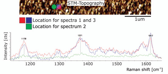
| Figure 9. TERS spectrum of malachite green obtained using the Innova IRIS at two different locations separated by <90nm indicated by the blue and green dots in the above SPM image. The first spectrum at location 1 is displayed in blue, the second second spectrum at location 2 in green, and the third spectrum back at location 1 is shown in red proving the sub-diffraction lateral resolution capabilities and reproducibility. | |
| After a topographic scan was taken, the tip was parked at the location indicated by the blue/red dot shown in the topographic data and a TERS spectrum was acquired. Under closed-loop control the tip was then moved to the location marked by the green dot and another Raman spectrum was taken. To verify that no sample damage occurred the tip was moved back to the original starting position and another spectrum was recorded. The intensity changes in the spectra between the two locations demonstrate that the resolution is indeed sub-wavelength and that no sample or tip damage occurred during the data acquisition. Lateral resolution for TERS is related to the active area of the signal enhancing tip and typically somewhere in the range of 10nm to 20nm. | |
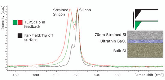
| Stress in materials can have a severe impact on device functionality and hence is an important parameter to know and control. Raman scattering is a good methodology for measuring stress in silicon devices by analyzing the shift of the first order Raman band at 520 cm-1. Unfortunately, the diffraction limit restricts those measurements to typically 1µm lateral resolution. Using TERS, one can extend those measurements to resolutions in the order of a few nanometers. | |
| Figure 10 shows a spectral measurement obtained on a model device consisting of a 70nm layer of strained silicon residing on top of an ultrathin barrier layer of BaOx followed by bulk Si. As the TERS tip approaches the sample, the increased signal from the strained Si-layer is readily apparent. This opens the door for further studies and a variety of applications on silicon devices. | |
 |
|
| Figure 10. Tip enhanced Raman spectrum of Si device with 70nm thick strained Si layer on ultrathin BaOx followed by bulk Si. The increased signal from the strained Si layer upon tip approach is readily apparent. Courtesy of D. Kosemura, Meiji University, Japan. | |
| Conclusion | |
| Co-localized AFM and Raman instrumentation allows researchers to interrogate samples using both scanning probe techniques and optical spectroscopy, yielding detailed information about nanoscale properties and composition. Diffraction-limited AFM-Raman experiments are straightforward as is the interpretation of data. TERS provides chemical information on the nanometer scale. | |
| TERS experiments are straightforward to execute but may require special consideration of the tip-sample interaction in the optical near-field for data interpretation. | |
| Download this Application Note as PDF | |
| References | |
| 1. G. Binnig, C. Quate, and Ch. Gerber, “Atomic Force Microscope,” Physical Review Letters 56 (1986): 930-33. | |
| 2. H. Kuzmany, Solid State Spectroscopy, 2nd edition, Springer: Heidelberg, 2009. | |
| 3. D. Harris and M. Bertolucci, Symmetry and Spectroscopy, Oxford University Press: New York, 1989. | |
| 4. S. Berweger, C. Neacsu, Y. Mao, H. Zhou, S. Wong, and M. Raschke, “Optical nanocrystallography with tip-enhanced phonon Raman spectroscopy,” Nature Nanotechnology 4 (2009): 469-99. | |
| 5. R. Saito, M. Hoffmann, G. Dresselhaus, A. Jorio, and M.S. Dresselhaus, “Raman spectroscopy of graphene and carbon nanotubes,” Advances in Physics 60, 3 (2011): 413-550. | |
| 6. E.H. Synge, “A suggested method for extending the microscopic resolution into the ultramicroscopic region,” Philosophical Magazine 6 (1928): 356-62. | |
| 7. A. Hartschuh, “Tip-Enhanced Near-Field Optical Microscopy,” Angewandte Chemie 47 (2008): 8178-91. | |
| 8. A. Downes, D. Salter, and A. Elfick, “Finite Element Simulations of Tip-Enhanced Raman and Fluorescence Spectroscopy,” Journal of Physical Chemistry B 110 (2006): 6692-98. | |
| 9. Z. Yang, J. Aizpurua, and H. Xu, “Electromagnetic fieldenhancement in TERS configurations,’ Journal of Raman Spectroscopy 40 (2009): 1343-48. | |
| 10. R. Stöckle, Y.Suh, V. Deckert, and R. Zenobi, “Nanoscale chemical analysis by tip-enhanced Raman spectroscopy,” Chemical Physical Letters 318 (2000): 131-36. | |
| 11. T. Ichimura, S.Fujii, P. Verma, T. Yano, Y.Inouye, and S. Kawata, “Subnanometric Near-Field Raman Investigation in the Vicinity of a Metallic Nanostructure,” Physical Review Letters 102 (2009): 186101. | |
| 12. W.H.J. Rensen, Ph.D. thesis, University of Twente (2002). | |
| 13. S.B. Kaemmer, Bruker Applications Note 133 (2011). | |
| 14. J. Steidtner and B. Pettinger, “Tip-enhanced Raman spectroscopy and microscopy on single dye molecules with15nm resolution,” Physical Review Letters 100 (2008): 236101. | |
| 15. C.C. Neascu, J. Dreyer, N. Behr, and M.B. Raschke, “Scanning probe Raman spectroscopy with single molecule sensitivity,” Physical Review B 73 (2006): 193403. | |
| 16. K. Domke and B. Pettinger, “Studying Surface Chemistry beyond the Diffraction Limit: 10 Years of TERS,” ChemPhysChem 11 (2010): 1365-73. | |
| 17. R. Ramos and M. Gordon, “Near-field artifacts in tip-enhanced Raman spectroscopy,” Applied Physics Letters 100 (2012): 213111. | |
| 18. I. De Wolf, “Micro-Raman spectroscopy to study local mechanical stress in silicon integrated circuits,” Semiconductor Science and Technology 11 (1996): 139-54. | |
|
By Stefan Kaemmer, Ph.D., Bruker Nano Surfaces ([email protected])
|
|
|
Become a Spotlight guest author! Join our large and growing group of guest contributors. Have you just published a scientific paper or have other exciting developments to share with the nanotechnology community? Here is how to publish on nanowerk.com. |
|