Showing Spotlights 137 - 144 of 252 in category All (newest first):
 In contrast to flexible electronics, which rely on bendable substrates, truly foldable electronics require a foldable substrate with a very stable conductor that can withstand folding, i.e. an edge in the substrate at the point of the fold, which develops creases, and the deformation remains even after unfolding. That means that, in addition to a foldable substrate like paper, the conductor that is deposited on this substrate also needs to be foldable. Researchers have now demonstrated a fabrication process for foldable graphene circuits based on paper substrates.
Aug 22nd, 2013
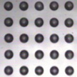 Graphene has a unique combination of properties that is ideal for next-generation electronics, including mechanical flexibility, high electrical conductivity, and chemical stability. Combine this with inkjet printing, already extensively demonstrated with conductive metal nanoparticle ink, and you get an inexpensive and scalable path for exploiting these properties in real-world technologies. Although liquid-phase graphene dispersions have been demonstrated, researchers are still struggling with sophisticated inkjet printing technologies that allow efficient and reliable mass production of high-quality graphene patterns for practical applications. Recent work has addressed these issues and proposes an approach to overcome these problems.
Aug 20th, 2013
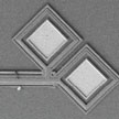 Semiconductor fabs are large, complex industrial sites with costs for a single facility approaching $10B. In this article we discuss the possibility of putting the entire functionality of such a fab onto a single silicon chip. We demonstrate a path forward where, for certain applications, especially at the nanometer scale, one might consider using a single chip approach for building devices, both integrated circuits and nano-electromechanical systems. Such methods could mean shorter device development and fabrication times with a significant potential for cost savings.
Aug 8th, 2013
 In addition to manipulating the charge or spin of electrons, another way to control electric current is by using the 'valley' degree of freedom of electrons. This novel concept is based on utilizing the wave quantum number of an electron in a crystalline material. Researchers now report the first demonstration of the generation, transport and detection of valley-polarized electrons in bulk diamond - a result which opens up new opportunities for quantum control in electronic devices.
Aug 5th, 2013
 Electronics will undergo revolutionary changes as the relatively novel disciplines of spintronics, nanoelectronics, and quantum computing come of age. A fundamental link between these fields can be established using molecular magnetic materials and, in particular, single-molecule magnets. Researchers have now demonstrated how to noninvasively graft a single-molecule magnet onto a carbon nanotube nanoelectromechanical system and probe the molecular nanomagnet with the carbon nanotube's mechanical motion.
Jul 19th, 2013
 Flexible electronics are all the rage these days. They promise an entirely new design tool like for instance, tiny smartphones that wrap around our wrists, and flexible displays that fold out as newspapers or large as a television; or photovoltaic cells and reconfigurable antennas that conform to the roofs and trunks of our cars. This article reviews the progress in single-walled CNT and graphene-based flexible thin-film transistors related to material preparation, fabrication technique and transistor performance control, in order to clarify the possible scale-up methods by which mature and realistic flexible electronics could be achieved.
Jun 5th, 2013
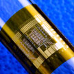
 For a transistor to work properly, it must contain impurity atoms - called dopants - replacing the silicon atoms at certain places in the device. Given that modern transistor are approaching the atomic scale, the exact location of a single dopant atom becomes critical in determining the device functionality. In a different context, single dopant atoms in semiconductors have now proved to be an excellent platform to encode quantum information. Therefore, the exact location of single dopant atoms is also crucial to future quantum computers based on silicon. A new technique allows the accurate location of a single dopant atom in a nanoscale device, after the device has been fabricated, and without damaging or altering any of its functionalities.
May 8th, 2013
 With all the rapid progress going on in research and commercialization of flexible and transparent electronics, the obvious question is not if, but when it will be possible to build a flexible and transparent truly high performance computer. A research team has now shown, for the first time, a generic batch fabrication process to obtain mechanically flexible and transparent mono-crystalline silicon (100) from bulk wafers. The researchers demonstrate a pragmatic pathway for a truly high performance computation systems on flexible and transparent platform.
Mar 1st, 2013
 Subscribe to our Nanotechnology Spotlight feed