Showing Spotlights 241 - 248 of 262 in category All (newest first):
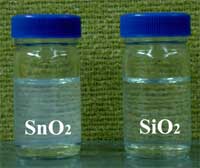 One of the newly emerging areas of semiconductor technology is the field of transparent electronics. These thin-film materials hold the promise of a new class of flexible and transparent electronic components that would be more environmentally benign than current electronics. Being able to print transparent circuits on low-cost, flexible, plastic substrates opens up the possibility of a wide range of new applications, ranging from windshield displays and flexible solar cells to clear toys and artificial skins and even sensor implants. It is likely that such flexible see-through structures will find wide uses in military, biosensing and consumer goods due to the advantages of high transparency and reliable electrical characteristics. However, the emerging transparent electronics technology is facing manufacturing problems: current fabricating processes do not separate the device manufacturing from material synthesis. The transparent electronic materials, which are largely inorganic oxides. are directly deposited on the device substrate under harsh conditions which may cause damage to the existing layer or flexible substrate. The etching of small dimension oxide multilayer is also difficult due to the low selectivity of the etching recipe. New research results demonstrate that nanofabrication techniques could solve these problems.
Apr 30th, 2007
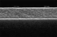
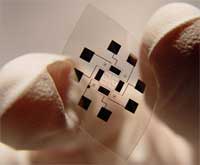 The fabrication of electronic devices on plastic substrates has attracted considerable recent attention owing to the proliferation of handheld, portable consumer electronics. Plastic substrates possess many attractive properties including biocompatibility, flexibility, light weight, shock resistance, softness and transparency. Achieving high performance electronics or sensors on plastic substrates is difficult, because plastics melt at temperatures above 120 degrees C. Central to continued advances in high-performance plastic electronics is the development of robust methods for overcoming this temperature restriction. Unfortunately, high quality semiconductors (such as silicon) require high growth temperatures, so their application to flexible plastics is prohibited. A group of researchers at the California Institute of Technology now showed that highly ordered films of silicon nanowires can be literally glued onto pieces of plastic to make flexible sensors with state-of-the-art sensitivity to a range of toxic chemicals. These nanowires are crystalline wires made out of doped silicon - the mainstay of the computer industry. By etching nanowires into a wafer of silicon, and then peeling them off and transferring them to plastic, they developed a general, parallel, and scalable strategy for achieving high performance electronics on low cost plastic substrates.
Apr 23rd, 2007
 Organic materials offer new electronic functionality not available in inorganic devices. Promising examples of novel characteristics in organic devices range from the memory effects observed in monolayers and polymer films to negative differential resistance devices. However, the integration of organic compounds within nanoscale electronic circuitry poses considerable challenges for materials physics and chemistry, and a detailed understanding of the conduction mechanisms, switching and memory is still lacking. With increasing research into very different material systems such as oxides, solid-state electrolytes, phase-change memory materials, it is becoming clear that electronic switching on the smallest length scale cannot be purely electronic phenomena. Rather, a motion of heavier constituents has to be involved that will in turn change the electronic properties. New work conducted at Bell Labs demonstrates the success of such a line of thought in molecular systems. The Bell scientists demonstrated a novel approach to creating and chemically modifying conducting electronic states in nanoscale molecular devices.
Apr 11th, 2007
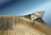
 In the future, wearable electronics will go far beyond just very small electronic devices. Not only will such devices be embedded on textile substrates, but an electronics device or system could become the fabric itself. Electronics textiles will allow the design and production of a new generation of garments with distributed sensors and electronic functions. Such e-textiles will have the revolutionary ability to sense, act, store, emit, and move (think biomedical monitoring functions or new man-machine interfaces) while leveraging an existing low-cost textile manufacturing infrastructure. Reporting a novel approach through the construction of all-organic wire electrochemical transistor devices (WECT) , researchers in Sweden show that textile monofilaments can be coated with continuous thin films of a conducting polymer and used to create microscale WECTs on single fibers. They also demonstrate inverters and multiplexers for digital logic. This opens an avenue for three-dimensional polymer micro-electronics, where large-scale circuits can be designed and integrated directly into the three-dimensional structure of woven fibers.
Apr 4th, 2007
 A few years ago it was discovered that the process of thermal inkjet printing can be applied to fabricate hard tissue scaffolds (such as bones) and, just recently, soft tissue with liquid biomaterials. Research is also underway to use inkjet printing for the fabrication of organic semiconductors, which, because of their low stability, will be targeted at one-time-only applications such as water purity testers. Compared to the research done with respect to organic materials, inkjet printing of inorganic materials for the formation of active devices is relatively rare. To date, only a handful of inorganic materials have been inkjet printed, primarily because of the difficulty in preparing inkjet-printable precursors. Current methods for the production of functional inorganic electronic devices are quite expensive because they require the sequential deposition, patterning, and etching of selected semiconducting, conducting, and insulating materials, involving multiple photolithography and vacuum-deposition processes. Now though, researchers have come up with a process for printable inorganic semiconductors, opening a route to the fabrication of high-performance and ultra low-cost electronics such as transparent electronics and thin film solar cells.
Mar 20th, 2007
 Nanoelectronics devices often are made by integrating dissimilar classes of semiconductors and various other disparate materials into one heterogeneous single system. The two primary modes of combining these materials - mechanical bonding and epitaxial growth processes - place stringent requirements on the ultimate scale or constituent materials of circuits. With mechanical bonding, there is a limited ability to scale to large areas (i.e., larger than the wafers) or to more than a few stacking layers; incompatibility with unusual materials (such as nanostructured materials) and/or low-temperature materials and substrates; challenging fabrication and alignment for the through-wafer electrical interconnects; demanding requirements for planar bonding surfaces; and bowing and cracking that can occur from mechanical strains generated by differential thermal expansion and contraction of disparate materials. Epitaxy avoids some of these problems but places severe restrictions on the quality and type of materials that can be grown. Using a process akin to the printing press, researchers have managed to bypass the need for epitaxial growth or wafer bonding to integrate wide ranging classes of dissimilar semiconducting nanomaterials onto substrates for the purpose of constructing heterogeneous, three dimensional electronics.
Feb 27th, 2007
 Gears, bearings, and liquid lubricants can reduce friction in the macroscopic world, but the origins of friction for small devices such as micro- or nanoelectromechanical systems (NEMS) require other solutions. Despite the unprecedented accuracy by which these devices are nowadays designed and fabricated, their enormous surface-volume ratio leads to severe friction and wear issues, which dramatically reduce their applicability and lifetime. Traditional liquid lubricants become too viscous when confined in layers of molecular thickness. This situation has led to a number of proposals for ways to reduce friction on the nanoscale, such as superlubricity and thermolubricity. Researchers in Switzerland now describe a resonance-induced superlubricity, which also occurs in many natural phenomena from biological systems to the motion of tectonic plates. This new method provides an efficient way to switch friction on and off at the atomic scale and, as a simple way of preventing mechanical damage without chemical contamination, could be of enormous importance for the development of NEMS.
Dec 20th, 2006
There is much discussion of molecules as components for future electronic devices and in recent years it has been possible to position single molecules in electrical junctions. Molecular and nanoscale structures have been shown to be capable of basic electronic functions such as rectification, negative differential resistance and single-electron transistor behavior. These observations show that molecular-electronic functions can be controlled through chemical manipulation. However, the contacts, the local environment and the temperature can all affect molecules' electrical properties. This sensitivity, particularly at the single-molecule level, may limit the use of molecules as active electrical components, and therefore it is important to design and evaluate molecular junctions with a robust and stable electrical response over a wide range of junction configurations and temperatures. A step in this direction, researchers in the UK now report an approach to monitor the electrical properties of single-molecule junctions, which involves precise control of the contact spacing and tilt angle of the molecule.
Dec 12th, 2006
 Subscribe to our Nanotechnology Spotlight feed