Showing Spotlights 225 - 232 of 262 in category All (newest first):
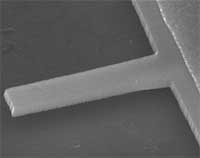
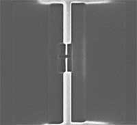 Yesterday we wrote about air bridges in nanotechnology fabrication. Today we show a practical example. Traditionally, electronic devices have been fabricated by top-down fabrication methods. Conducting polymers, for instance, have been synthesized as micro- and nanoscale fibers, tubes and wires for more than 10 years now. More recently, nanowires have been integrated into electronic circuits, making possible the development of devices such as polymer nanowire chemical sensors with superior performance. What most of these fabrication techniques have in common is that they are template-based (e.g. lithography or DNA templates) or depend on specialized fiber forming techniques such as electrospinning. However, as electronic components become smaller and smaller it is increasingly more difficult to use existing methods of fabrication. New methods must be developed. A group of researchers in Australia have demonstrated a technique for growing ordered polymer nanowires within a pre-patterned electronic circuit such that electrical contacts to the nanowires are made in situ during the growth procedure, avoiding the time-consuming and challenging task of manipulating nanowires into position and making electrical contacts post-synthesis.
Sep 27th, 2007
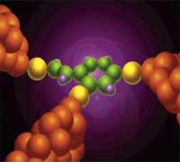 Transistors are the fundamental building blocks of our everyday modern electronics; they are the tiny switches that process the ones and zeroes that make up our digital world. Transistors control the flow of electricity by switching current on or off and by amplifying electrical signals in the circuitry that governs the operation of our computers, cellular phones, iPods and any other electronic device you can think of. The first transistor used in commercial applications was in the Regency TR-1 transistor radio, which went on sale in 1954 for $49.95, that's over $375 in today's dollars (for everyone in the iPod generation - watch this fascinating 1955 video clip artifact how the first transistor radio was hand built). While the first transistors were over 1 centimeter in diameter, the smallest transistors today are just 30 nanometers thick - three million times smaller. This feat would be equivalent to shrinking the 509-meter tall Taipei 101 Tower, currently the tallest building in the world, to the size of a 1.6 millimeter tall grain of rice. The 32nm microprocessor Intel plans to introduce in 2009 will pack a whopping 1.9 billion transistors. However, current microprocessor technology is quickly approaching a physical barrier. Switching the current by raising and lowering the electron energy barrier generates heat, which becomes a huge problem as device densities approach the atomic limit. An intriguing - and technologically daunting - alternative would be to exploit the wave nature of the electron, rather than its particle properties, to control current flow on the nanoscale. Such a device, called the Quantum Interference Effect Transistor (QuIET), has been proposed by researchers in Arizona. This device could be as small as a single benzene molecule, and would produce much less heat than a conventional field effect transistor.
Sep 25th, 2007
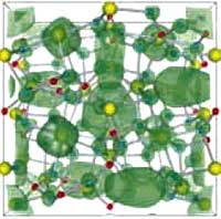
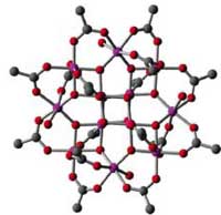 Lithium-ion (Li-ion) batteries are a type of rechargeable battery commonly used in consumer electronics. They are currently one of the most popular types of battery for portable electronics, with one of the best capacity-to-weight ratios, no memory effect, and a slow loss of charge when not in use. Lithium is useful in batteries because of its lightness (it is the lightest metal) and because of the high voltage of the redox reaction between Li and Li+. In lithium ion batteries, a layered compound - lithium copper oxide or or lithium nickel oxide - is utilized as a cathode. Although this material can provide high capacity, its charging/discharging rates are slow because these processes include the absorption/desorption of lithium in the cathode. Recently, organic radical batteries have been developed as a new type of rechargeable battery, in which organic radical polymers are utilized as a cathode active material. They achieved a very fast chargeable/dischargeable rate, though their capacities are lower than those of the lithium ion batteries. A lot of research has gone into fabricating lithium batteries that achieve both high capacity and fast charging/discharging. Researchers in Japan came up with a completely new idea - the molecular cluster battery - where the cathode active material is a well-known manganese molecular cluster that is stable and insoluble to most solvents and exhibits a multi-step redox reaction. Although the battery was rechargeable, in early experiments the fast charging�??discharging was not yet achieved due to the chemical decomposition of the cluster. Nevertheless, this is a first step that opens up a new branch of research into high-performance rechargeable molecular cluster batteries.
Sep 20th, 2007
 Apart from buying a new computer every year it seems you need to upgrade your old machine on a regular basis to keep pace with ever bigger software packages and image files. Apart from the hassle of having to perform major surgery on your computer, these upgrades cost money. But, what if these upgrades were no longer necessary? What if your desktop computer came standard with the ability to store more data than you could ever possibly need and was able to function at unbelievable speeds? This would be too good to be true, right? Besides, who has the space for such a megacomputer. Well, imagine that this megacomputer could be packaged as a smaller device than current laptops, and cost only a fraction of today�??s prices? This sounds like hard core science fiction, but like so many radical science fiction ideas - the real thing might happen sooner than you think. As chip designers are nearing the physical limits of Moore's law (some say that the exponential increase in the cost of semiconductor production will most likely stop the current miniaturization trend before its physical limits are reached), scientists around the globe are working hard on developing the field of molecular electronics. An interdisciplinary science that includes physics, chemistry, nanotechnology, materials science and even biology, molecular electronics involves using molecular building blocks in the manufacture of electronic components. Driven by a growing interest in alternative concepts, like the integration of molecules as carriers of an electronic function, the electronics industry is poised to take the crucial step of integrating molecular devices into electronic circuits.
Sep 17th, 2007
 Many of us don't like to admit it, but televisions are an important part of our lives. Technology has improved the quality and convenience of TVs and has given us a whole new set of choices - high definition, plasma, and liquid crystal displays. With an estimated 66 million sets to be sold this year, flat-screen LCD televisions are the most popular choice. Much of the reason behind the popularity of these high-tech wonders is the decrease in price that happens with most cool technology - a few years after they have been on the market. But, for the popular LCD TV, a shortage of a key compound used to produce LCDs may force manufacturers to raise prices. Electronics suppliers are facing a shortage of the rare metal indium, a co-product of zinc mining. Indium is a rare, malleable and easily fused metal, similar to aluminum, which is used to make indium tin oxide (ITO), the standard transparent electrode used in nearly all flat panel displays and microdisplays. Indium is expensive and scarce and demand is increasing. According to Displaybank, the demand for indium was 861 tons in 2006 and may reach nearly 2000 tons by 2011. Five years ago, indium was about $100/ kg; now it costs $800/kg. Displaybank expects the total sales of indium in 2007 to be $533 million. But, geologists say the cost of indium may not matter soon, because the earth's supply of it could be gone in four years. This could put a serious damper on that 52" LCD screen you've been dreaming about. Fortunately, with the help of nanotechnology, a team of scientists in Japan have developed a new material that may replace the need for indium in LCD production.
Sep 14th, 2007
 In his famous 1959 speech "Plenty of Room at the Bottom", Richard Feynman offered a prize of $1000 "to the first guy who makes an operating electric motor - a rotating electric motor which can be controlled from the outside and, not counting the lead-in wires, is only 1/64 inch cube." Feynman had hoped his reward would stimulate some new fabrication technology but he was quite consternated when one year later, Bill McLellan, using amateur radio skills, built the motor with his hands using tweezers and a microscope (and many, many hours of fiddling around). McLellan's 2000 rpm motor weighed 250 micrograms and consisted of 13 parts. In the almost 50 years since, not only has the field of microelectromechanical systems (MEMS) caught up with Feynman's bet and achieved commercial production capabilities of motors many times smaller than McLellan's, but researchers have begun exploring another level of miniaturization - nanoelectromechanical systems (NEMS). Efficient actuation, the creation of mechanical motion by converting various forms of energy to rotating or linear mechanical energy, is an important - and today still frustrating - issue in designing NEMS. Research on building functional nanoscale electromechanical systems is well underway, as just demonstrated with another achievement by scientists at Caltech - the place where Feynman gave his speech and McLellan's motor still is on display.
Aug 27th, 2007
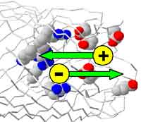 Ion channels are proteins with a hole down their middle that are the gatekeepers for cells. Ion channels control an enormous range of biological function in health and disease. In channels with a diameter greater than 100 nm, the interaction between the channel wall and electrolyte solution hardly affects the flow of ions. When the channel diameter enters the the below-10 nm range, things change dramatically, however. Then, the interaction between the solution and channel wall starts to dominate ionic flow and ion transport through such narrow, nano-scaled channels is dominated by electrostatics. The same is true for biological ion channels where charged amino residues in the selectivity filter determine the ionic flow through the channel, along with the dielectric charge on the channel wall, and the concentrations and potential in the bulk solution. The role electrostatics play in biological pores has been confirmed by numerous mutation studies where amino acids residues in the selectivity filter were replaced by others. Ion channels have simple enough structure that they can be analyzed with the usual tools of physical science. With that analysis in hand, researchers are trying to design practical machines that use ion channels. By exploiting the electrostatics in nanochannels a group of US and Dutch scientists managed to make a diode. Like a solid-state diode allows current flow in one direction, the ionic equivalent they designed can be used to direct the flow of ions across a membrane that separates two electrolyte solutions. Now that they know how to manipulate the ion selectivity in these devices, they hope to be able one day to selectively amplify currents carried by individual chemical species - a stunning prospect for molecular nanoelectronics.
Aug 21st, 2007
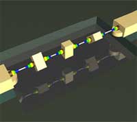 In the good old days, say 5,000 years ago, a bearing was simply the placement of tree trunks under the huge stone blocks that your worker army used to construct a pyramid. Since then, bearings have become a bit more sophisticated and are an essential part of much of today's machinery. Consequently, many kinds of bearings have been developed to suit particular purposes - sliding, rolling, fluid, or magnetic bearings, to name a few major categories. Bearings are now widely used for instance to reduce friction between shafts and axles or absorb the weight placed on moving parts and they are found in applications ranging from automobiles, trains and airplanes, computers, construction equipment, machine tools, to ceiling fans and roller skates. The same way that bearings have become an integral part of our modern world, they will also play an important role in the extremely miniaturized micro- and nanodevices of the future. Engineers will just have to come up with ingenuous ways to construct bearings at the nanoscale. Carbon nanotubes (CNTs) offer one possibility. Researchers have demonstrated that the relative displacements between the atomically smooth, nested shells in multiwalled carbon nanotubes (MWCNTs) can be used as a robust nanoscale motion-enabling mechanism. Even better, a group in Switzerland has demonstrated batch fabrication of such CNT bearings is possible.
Aug 17th, 2007
 Subscribe to our Nanotechnology Spotlight feed