Showing Spotlights 209 - 216 of 252 in category All (newest first):
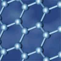
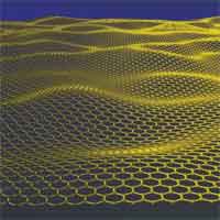 There has been quite a buzz about graphene, a single atomic layer thick, plane of carbon atoms arranged in a honeycomb lattice. Discovered only in 2004, graphene exhibits many exotic properties and currently is considered the most exciting new material system among nanotechnology researchers. This rising star in material science exhibits remarkable electronic properties that qualify it for applications in future optoelectronic devices. In a first experimental study of the thermal conductivity of single-layer graphene, researchers found that on top of many unique electronic properties, graphene also is an extraordinary good heat conductor. Measurements revealed that graphene's near room temperature thermal conductivity, which is in the range from 3500-5300 W/mK, is much higher than that of diamond, the best bulk crystal heat conductor. It appears that the thermal conductivity of graphene is larger than conventionally accepted experimental values reported for individual suspended carbon nanotubes (CNTs) and corresponds to the upper bound of the highest values reported for single-wall CNT bundles. The superb thermal conduction property of graphene is beneficial for its proposed electronic applications and establishes graphene as an excellent material for thermal management also in optoelectronics, photonics and bioengineering.
Feb 21st, 2008
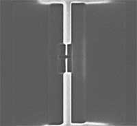
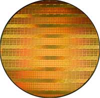 Due to their exceptional electronic and mechanical properties, as well as their nanoscale size, carbon nanotubes (CNTs) could become the active electronic elements in addressing next generation electronic requirements for which silicon is not a solution. Already, it has been shown extensively that semiconducting CNTs can be made into electronic components such as transistors and switches. Their thermal, mechanical, chemical stability, and large current-carrying capacity make CNTs attractive for applications not only in in electrical interconnects but also field-effect transistors, cold cathode field emitters, and sensors. Some of the problems in developing CNT-based electronic devices have to do with building reliable interconnections between CNTs and external electrical and mechanical systems and in developing a reliable fabrication batch process to allow for industrial-scale mass production that supports the direct manipulation and placement/growth of CNTs at specific locations. Pointing to a possible solution, researchers now have demonstrated controllable and simultaneous wafer-scale assembly of CNT networks by dielectrophoresis.
Feb 18th, 2008
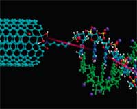 DNA, the blueprint of life, and electronics seem to be two completely different things but it appears that DNA could offer a solution to many of the hurdles that need to be overcome in further scaling down electronic circuits beyond a certain point. The reason why DNA could be useful in nanotechnology for the design of electric circuits is the fact that it actually is the best nanowire in existence - it self-assembles, it self-replicates and it can adopt various states and conformations. Not surprisingly, performing reliable experiments on a single oligo-DNA molecule is an extremely delicate task as partly contradicting research reports demonstrate: Different DNA transport experiments have shown that DNA may be insulating, semiconducting, or metallic. Among the numerous factors that could impact the results are the quality of the DNA-electrode interface, the base pair, the charge injection into the molecule, or environmental effects such as humidity or temperature. Researchers have now demonstrated a novel carbon nanotube-based nanoelectronic platform as proof of concept that single DNA molecules can be detected. This novel detection technique is based on change in electrical conductance upon selective hybridization of the complementary target DNA with the single stranded probe attached to the system. The single-stranded sequence-specific probe DNA whose ends are modified with amine is attached between two carbon nanotubes/nanowires using dielectrophoresis (DEP). This platform can be used for understanding how electrical charge moves through DNA which could help researchers understand and perhaps develop a technique for reversing the damage of DNA done by oxidation and mutation.
Dec 28th, 2007
 As a critical component of optoelectronic devices, transparent conductive coatings pervade modern technology. The most widely used standard coating is indium tin oxide (ITO), used in nearly all flat panel displays and microdisplays. Causing problems for manufacturers, though, Indium is expensive and scarce and demand is increasing. From the depressed levels of $60/kg in 2002, indium prices rose to over $1,000/kg during the summer of this year. Recently, prices have fallen back to between $400-$500/kg. But, geologists say the cost of indium may not matter soon, because the earth's supply of this element could be gone within just a few years. In addition to the limited availability of Indium there are other reasons that make ITO and other metal oxides such as FTO (fluorine tin oxide) increasingly problematic for electronics manufacturers: the instability of these metal oxides in the presence of acid or base; their susceptibility to ion diffusion into polymer layers; their limited transparency in the near-infrared region; and lastly, the current leakage of FTO devices caused by FTO structure defects. This has made the search for novel transparent electrode materials with good stability, high transparency and excellent conductivity a crucial goal for optoelectronic researchers. Recent work by researchers in Germany exploits ultra-thin transparent conductive graphene films as window electrodes in solar cells.
Dec 17th, 2007
 We have written plenty of Spotlights so far on carbon nanotubes and nanoelectronics. For instance, carbon nanotube (CNT) transistors have the potential to outperform state-of-the-art silicon devices. Researchers around the world have been working for years on advances at the device level, things like switches and wires and optimizing individual CNT transistors. More recently, scientists have begun to integrate nanotechnology-based materials and devices into larger systems - a crucial step in getting nanotechnology from the lab to the fab. Last year, for instance IBM reported to have built the first complete electronic integrated circuit around a single carbon nanotube (An integrated logic circuit assembled on a single carbon nanotube). Researchers in California have now reported another step towards showing nanoelectronics in systems: They have developed the world's first working radio system that receives radio waves wirelessly and converts them to sound signals through a nano-sized detector made of CNTs. Although this is only the demonstration of a single critical component (the CNT as demodulator) of an entire radio system, it is entirely possible that at some point in the future all components of a working radio could be nanoscale, thus allowing a truly nanoscale wireless communications system (apart from the magnitude of the technological achievement, this is probably great news for surveillance freaks, not so much for privacy advocates).
Oct 29th, 2007
 Nanoelectronics deals with functional electron devices, such as transistors, in the nanoscale range size. As the name implies, nanoelectronics runs on electricity, i.e. the transport of electrons. Another approach to creating faster,smaller and more energy-efficient electronics is to move the field of optical information processing towards the nanoscale. Optical nanoelectronics will work with light instead of electron transport. Here the usual circuit elements such as inductors, capacitors and resistors could be created in order to operate using infrared or visible light. Using nanotechnology, researchers are able to create structures that could operate on the same or smaller scale as the wavelength of light (the wavelength of visible light is roughly between 400 and 700 nanometers). Going beyond 'conventional' nanoelectronics, researchers have now proposed a form of optical circuitry in which a network of subwavelength nanoscale metamaterial structures and nanoparticles may provide a mechanism for tailoring, patterning, and manipulating optical electric fields in a subwavelength domain, leading to the possibility of optical information processing at the nanometer scale.
Oct 16th, 2007
 Yesterday we wrote about air bridges in nanotechnology fabrication. Today we show a practical example. Traditionally, electronic devices have been fabricated by top-down fabrication methods. Conducting polymers, for instance, have been synthesized as micro- and nanoscale fibers, tubes and wires for more than 10 years now. More recently, nanowires have been integrated into electronic circuits, making possible the development of devices such as polymer nanowire chemical sensors with superior performance. What most of these fabrication techniques have in common is that they are template-based (e.g. lithography or DNA templates) or depend on specialized fiber forming techniques such as electrospinning. However, as electronic components become smaller and smaller it is increasingly more difficult to use existing methods of fabrication. New methods must be developed. A group of researchers in Australia have demonstrated a technique for growing ordered polymer nanowires within a pre-patterned electronic circuit such that electrical contacts to the nanowires are made in situ during the growth procedure, avoiding the time-consuming and challenging task of manipulating nanowires into position and making electrical contacts post-synthesis.
Sep 27th, 2007
 Transistors are the fundamental building blocks of our everyday modern electronics; they are the tiny switches that process the ones and zeroes that make up our digital world. Transistors control the flow of electricity by switching current on or off and by amplifying electrical signals in the circuitry that governs the operation of our computers, cellular phones, iPods and any other electronic device you can think of. The first transistor used in commercial applications was in the Regency TR-1 transistor radio, which went on sale in 1954 for $49.95, that's over $375 in today's dollars (for everyone in the iPod generation - watch this fascinating 1955 video clip artifact how the first transistor radio was hand built). While the first transistors were over 1 centimeter in diameter, the smallest transistors today are just 30 nanometers thick - three million times smaller. This feat would be equivalent to shrinking the 509-meter tall Taipei 101 Tower, currently the tallest building in the world, to the size of a 1.6 millimeter tall grain of rice. The 32nm microprocessor Intel plans to introduce in 2009 will pack a whopping 1.9 billion transistors. However, current microprocessor technology is quickly approaching a physical barrier. Switching the current by raising and lowering the electron energy barrier generates heat, which becomes a huge problem as device densities approach the atomic limit. An intriguing - and technologically daunting - alternative would be to exploit the wave nature of the electron, rather than its particle properties, to control current flow on the nanoscale. Such a device, called the Quantum Interference Effect Transistor (QuIET), has been proposed by researchers in Arizona. This device could be as small as a single benzene molecule, and would produce much less heat than a conventional field effect transistor.
Sep 25th, 2007
 Subscribe to our Nanotechnology Spotlight feed