Showing Spotlights 233 - 240 of 262 in category All (newest first):
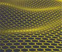 Carbon comes in many different forms, from the graphite found in pencils to the world's most expensive diamonds. In 1980, we knew of only three basic forms of carbon, namely diamond, graphite, and amorphous carbon. Then, fullerenes and carbon nanotubes were discovered and all of a sudden that was where nanotechnology researchers wanted to be. Recently, though, there has been quite a buzz about graphene. Discovered only in 2004, graphene is a flat one-atom thick sheet of carbon. Existing forms of carbon basically consist of sheets of graphene, either bonded on top of each other to form a solid material like the graphite in your pencil, or rolled up into carbon nanotubes (think of a single-walled carbon nanotube as a graphene cylinder) or folded into fullerenes. Physicists had long considered a free-standing form of planar graphene impossible; the conventional wisdom was that such a sheet always would roll up. Initially using such high-tech gadgets like pencils and sticky tape to strip chunks of graphite down to layers just one atom thick, the process has now been refined to involve more expensive instruments such as electron beam and atomic force microscopes. Despite being isolated only three years ago, graphene has already appeared in hundreds of papers. The reason scientists are so excited is that two-dimensional crystals (it's called 2D because it extends in only two dimensions - length and width; as the material is only one atom thick, the third dimension, height, is considered to be zero) open up a whole new class of materials with novel electronic, optical and mechanical properties.
Aug 8th, 2007
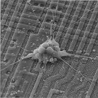
 One of the many fascinating concepts in nanotechnology is the vision of molecular electronics. If realized, the shift in size from even the smallest computer chip today would be staggering - a quantum leap, so to speak (literally). Look at it this way: a single drop of water contains more molecules than the billions and billions of silicon chips ever produced. Molecular electronics engineers of tomorrow might use individual molecules to perform the functions in an electronic circuit that are performed by semiconductor devices today. Don't get your hopes up, though, that your next iPod will be truly nano. Scientists today are still struggling with the most basic requirements for molecular electronics, for instance, how to precisely and reliably position individual molecules on a surface. DNA-based nanostructuring is one approach that could lead to promising results. It has already been shown that DNA could be used to structure nanoscale surfaces. Now, a team in Germany has demonstrated that nanoscale objects of very different size can be deposited simultaneously and site-selectively onto DNA-displaying surfaces, based on sequence-specific DNA-DNA duplex formation.
Aug 6th, 2007
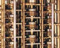 Finding out how much power all the computers in the U.S., not to mention the world, are using seems to be an impossible task. We tried. The latest data from the Department of Energy (DoE) for household computer use is from 2001, for office use, from 1999. This is strange because when you do some back of the envelope calculations you arrive at some pretty staggering numbers. An estimated 1 billion computers in 2008 will use some 200 billion kWh of electricity (that's roughly what all households in New York City combined use over five years), generating about 127 million tonnes of CO2 in the process. And that's just for desktop and laptop computers, not including peripherals or the billions of chips used in other electronic devices. Researchers are now proposing to build a fully mechanical computer based on nanoelectromechanical (NEMS) components that would use considerably less energy. Inspired by a classical mechanical computer design from 200 years ago, the main motivation behind constructing such a computer is threefold: (1) mechanical elements are more robust to electromagnetic shocks than current dynamic random access memory (DRAM) based purely on complimentary metal oxide semiconductor (CMOS) technology, (2) the power dissipated can be orders of magnitude below CMOS and (3) the operating temperature of such an NMC can be an order of magnitude above that of conventional CMOS. Today, such a mechanical computer is only a hypothetical device. However, any effort to reduce the power consumption of computers, and not increase them as happens with every new chip generation, seems like a worthwhile effort.
Jul 25th, 2007
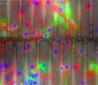 Just a few days ago we ran a Spotlight on nanobionics that addressed some of the issues of bridging the interface between electronics and biology. Today we'll take a look at some leading edge research in the field of neural engineering - an emerging discipline that uses engineering techniques to investigate the function and manipulate the behavior of the central or peripheral nervous systems. Neural engineering is highly interdisciplinary and relies on expertise from computational neuroscience, experimental neuroscience, clinical neurology, electrical engineering and signal processing of living neural tissue, and encompasses elements from robotics, computer engineering, neural tissue engineering, materials science, and nanotechnology. In order for neural prostheses to augment or restore damaged or lost functions of the nervous system they need to be able to perform two main functions: stimulate the nervous system and record its activity. To do that, neural engineers have to gain a full understanding of the fundamental mechanisms and subtleties of cell-to-cell signaling via synaptic transmission, and then develop the technologies to replicate these mechanisms with artificial devices and interface them to the neural system at the cellular level. The first steps toward precise, informative and biocompatible neural interfaces have been made already.
Jul 24th, 2007
 In case you are not old enough to remember the TV series The Six Million Dollar Man during the 1970s, the show was about an astronaut, Steve Austin, who got severely injured during a crash and became a guinea pig for bionics experiments by the CIA. In an operation that cost six million dollars, his right arm, both legs and the left eye are replaced by bionic (cybernetic) implants that vastly enhanced his strength, speed and vision. Never mind Hollywood, though, but bionics - a word formed from biology and electronics - has become a serious research field. In particular the development of artificial muscles is progressing rapidly. Nature's solution to producing fast contracting muscles is to use nanotechnology. The challenge for scientists is to mimic the intricacy of natural muscle in their artificial-muscle systems. As material scientists and engineers delve into the nanodomain, the boundaries between electronics and biology become fuzzy and this is exactly what they want: a seamless transition between the hard world of electronics and the soft world of biology.
Jul 17th, 2007
 Nanoimprinting lithography (NIL) is a simple pattern transfer process that is emerging as an alternative nanopatterning technology to traditional photolithography. NIL allows the fabrication of two-dimensional or three-dimensional structures with submicrometer resolution and the patterning and modification of functional materials. A key benefit of nanoimprint lithography is its sheer simplicity. There is no need for complex optics or high-energy radiation sources with a nanoimprint tool. There is no need for finely tailored photoresists designed for both resolution and sensitivity at a given wavelength. The simplified requirements of the technology allow low-cost, high-throughput production processes of various nanostructures with operational ease. NIL already has been applied in various fields such as biological nanodevices, nanophotonic devices, organic electronics, and the patterning of magnetic materials. Researchers at Berkeley have taken this process one step further by demonstrating that direct nanoimprinting of metal nanoparticles enables low temperature metal deposition as well as high-resolution patterning. This approach has substantial potential to take advantage of nanoimprinting for the application in ultralow cost, large area printed electronics.
Jun 27th, 2007
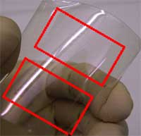 Thin-film transistors (TFTs) and associated circuits are of great interest for applications including displays, large-area electronics and printed electronics (e.g. radio-frequency identification tags - RFID). Well-established TFT technologies such as amorphous silicon and poly-silicon are well-suited for many current applications - almost all mobile phone color screens use them - but face challenges in extensions to flexible and transparent applications. In addition, these TFTs have modest carrier mobilities, a measure of the velocity of electrons within the material at a given electric field. The modest mobility corresponds to a modest operating speed for this class of TFTs. Organic TFTs are generally better suited for flexible applications, and can be made transparent. However, mobilities in organic TFTs are generally quite low, restricting the speed of operation and requiring relatively large device sizes. Researchers at Purdue University, Northwestern University, and the University of Southern California now have reported nanowire TFTs that have significantly higher mobilities than other TFT technologies and therefore offer the potential to operate at much higher speeds. Alternatively, they can be fabricated using much smaller device sizes, which allows higher levels of integration within a given chip area. They also provide compatibility with a variety of substrates, as well as the potential for room-temperature processing, which would allow integration of the devices with a number of other technologies (e.g. for displays).
Jun 12th, 2007
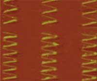
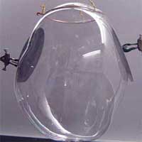 One of the most common methods of film manufacture is Blown Film Extrusion. The process, by which most commodity and specialized plastic films are made for the packaging industry, involves extrusion of a plastic through a circular die, followed by "bubble-like" expansion. The resulting thin tubular film can be used directly, or slit to form a flat film. Nanoscientists now have found a way to use this very common and efficient industrial technology to potentially solve the problem of fabricating large-area nanocomposite films. Currently, the problems with making thin film assemblies are either the production cost of using complex techniques like wet spinning or the unsatisfactory results of unevenly distributed and lumping nanoparticles within the film. The new bubble film technique results in well-aligned and controlled-density nanowire and carbon nanotubes (CNTs) films over large areas. These findings could finally open the door to affordable and reliable large-scale assembly of nanostructures.
May 31st, 2007
 Subscribe to our Nanotechnology Spotlight feed