Showing Spotlights 161 - 168 of 262 in category All (newest first):
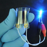 High-performance flexible power sources have gained attention as they enable the realization of next-generation bendable, implantable, and wearable electronic systems. Numerous approaches to fabricate flexible energy sources have been developed, ranging from various designs for transparent electrodes to entire nanogenerators for self-powered devices and systems. In the past, researchers have tried to design flexible batteries with compliant materials in order to enhance the mechanical flexibility such as organic materials or nano/micro structured inorganic materials mixed with polymer binders. However, these organic materials have a low specific power density due to binder space and they generally have shown low performance for operating flexible devices such as bendable displays. In a new study, researchers have fabricated an all-solid-state bendable lithium-ion battery (LIB) structured with high-density inorganic thin films using a new universal transfer approach, which enables the realization of diverse flexible LIBs regardless of electrode chemistry.
Aug 7th, 2012
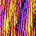 Quantum rings show unique electronic, magnetic and optical properties. These unique properties make them attractive for various applications such as magnetic memory and systems for future quantum computers. To be used in practical applications, however,the quantum rings need to be fabricated in a controlled fashion. So far, the fabrication of laterally ordered quantum rings has not been reported. Now, though, researchers have demonstrated a fabrication method to obtain large scale ordered quantum rings. The quantum rings can be simply created by partially capping quantum dots. The key to fabricating ordered quantum rings is to create ordered quantum dots.
Jun 21st, 2012
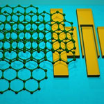 Gallium Nitride (GaN) is a semiconductor material commonly used in bright light-emitting diodes since the 1990s, which are now found in traffic lights and solid-state lighting. Thanks to its wide band gap, this very hard semiconductor material also finds applications in optoelectronic, high-power and high-frequency devices. However, a severe problem that afflicts high-power GaN electronic and optoelectronic devices is self-heating and the difficulties of heat removal. Researchers have now found an unusual solution for the thermal management problem of gallium-nitride technology: They demonstrated that thermal management of GaN transistors can be substantially improved via introduction of alternative heat-escaping channels implemented with graphene multilayers.
May 10th, 2012
 Graphene is an excellent conductor of heat and might be an ideal material for thermal management in nanoelectronics. In field-effect transistors or interconnects most of the heat propagates directly below the graphene channel in the direction of the heat sink, that is, the bottom of a silicon wafer. For this reason, the highly thermally resistive silicon layers act as a thermal bottleneck, preventing the full utilization of graphene's excellent intrinsic properties. The breakdown current density in typical graphene devices is a hundred times larger than the fundamental limit in metals, which is set by electromigration. Researchers wanted to see if we can push the breakdown current density in graphene even further by better removal of dissipated heat. They managed to do it with the help of high-quality synthetic diamond. The graphene transistors or interconnects on synthetic diamond can sustain current densities which are a thousand times larger than in metals.
Feb 20th, 2012
 For years it has been known that scaling bulk silicon transistors would be extremely challenging, if not impossible, when lengths close in on 15 nm. Already, attention has turned to 3D transistor design and silicon-on-insulator (SOI) devices to improve the scalability of silicon technology. Carbon nanotube (CNT) transistors have been touted as a possible replacement for silicon devices but the crucial question so far has been if CNT transistors can offer performance advantages over silicon at sub-10 nm lengths? New experimental results from IBM Research are indicating that the answer is 'yes'. The findings by the research team defied the theoretical projections and exhibited encouraging performance for a device with a 9 nm channel length.
Feb 9th, 2012
 Apart from graphene, other two-dimensional structures are also known to have unique properties which researchers are eager to exploit for novel nanotechnology applications in nanoelectronics and sensor or energy storage technology. Particular interest has been on semiconducting materials, such as molybdenum disulfide (MoS2), an abundant material in nature, which exhibits the unique physical, optical and electrical properties correlated with its single-layer atomic layer structure. Researchers have now fabricated a mechanically exfoliated single-layer MoS2 based phototransistor and investigated its electric characteristics in detail. These new findings show that, when compared with a 2D graphene-based device, the single-layer MoS2 phototransistor exhibits a better photoresponsivity.
Feb 3rd, 2012
 Thermal interface materials (TIMs) are essential ingredients of thermal management. TIMs are applied between the heat source, e.g. computer chips, and heat sinks and their function is to fill the voids and grooves created by imperfect surface finish of mating surfaces. Conventional TIMs filled with thermally conductive particles require high volume fractions of filler particles. But now, researchers have achieved a record enhancement of the thermal conductivity of TIMs by addition of an optimized mixture of graphene and multilayer graphene. The thermal conductivity of the epoxy matrix material was increased by an impressive factor of 23 at the 10 volume % of graphene loading. The epoxy-graphene composite preserved all the properties required for industrial TIM applications.
Jan 30th, 2012
 Lipids are the main component of the outermost membrane of cells. Their role is to seperate the inner and outer media of the cell and prevent any ionic current between these two media. Because of this last property, lipid layers can be thought of as good ultra-thin insulators that could be used in the development of electronic devices. So far though, because of their inherent instability in air, their use in advanced processes has been limited. This might change, though, since researchers in France have shown the possibility to stabilize by polymerization a lipid monolayer with a thickness of 2.7 nm directly at the surface of H-terminated silicon surface therefore opening a whole new world of possibilities of the use of these layers. Now, they reported the electrical performance of stabilized lipid monolayers on H-terminated silicon.
Oct 27th, 2011
 Subscribe to our Nanotechnology Spotlight feed