| Posted: Feb 03, 2012 |
Molybdenite-based phototransistor shows faster photoresponsivity than a graphene-based device |
| (Nanowerk Spotlight) Apart from graphene, other two-dimensional (2D) structures are also known to have unique properties which researchers are eager to exploit for novel nanotechnology applications in nanoelectronics and sensor or energy storage technology (read more in our Nanowerk Spotlight: "Graphene was only the beginning; now MAX phases get two-dimensional as well"). |
| Particular interest has been on semiconducting materials, such as molybdenum disulfide (MoS2), an abundant material in nature, which exhibits the unique physical, optical and electrical properties correlated with its single-layer atomic layer structure (read more: "A new transistor: Thinner than silicon and better than graphene"). |
| In new work, reported in a recent issue of ACS Nano ("Single-Layer MoS2 Phototransistors"), researchers have now fabricated a mechanically exfoliated single-layer MoS2 based phototransistor and investigated its electric characteristics in detail. |
| "Our findings show that, when compared with a 2D graphene-based device, the single-layer MoS2 phototransistor exhibits a better photoresponsivity," Hua Zhang, an Associate Professor in the School of Materials Science and Engineering at Nanyang Technological University (NTU), tells Nanowerk. "Overall, the unique characteristics, such as incident-light control, prompt photoswitching, and good photoresponsivity, of the single-layer MoS2 phototransistor are encouraging results. We hope it will lead to the fabrication the optoelectronic devices based on single atomic layer semiconductors by a facile and low-cost mechanic exfoliation method." |
| For their experiments, the NTU team deposited the single-layer MoS2 onto a Si/SiO2 substrate using the scotch-tape based mechanical exfoliation method – along the lines of how Andre Geim and Kostya Novoselov got started fabricating the first samples of graphene. The height of the single-layer MoS2 measured by AFM is ca. 0.8 nm, which, according to Zhang, is consistent with the previous theoretical and experimental results. |
| Using a photolithography technique, the researchers fabricated a MoS2 FET device where two titanium/gold electrodes and 300 nm SiO2 on Si were used as the source, drain, and back gate, respectively. |
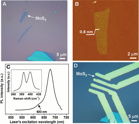 |
| (A) Optical microscopy image and (B) AFM image of single-layer MoS2. (C) PL and Raman (inset) spectra of single-layer MoS2. (D) Optical image of FET device made by single-layer MoS2 in (A, B). (Reprinted with permission from American Chemical Society) |
| "Photocurrent generation and annihilation of our phototransistor can be switched within ca. 50 ms" says Zhang. "Such prompt photoswitching behavior, controllable by the incident light, exhibits stable characteristics." |
| He adds, though, that the response rate of photocurrent in the team's single-layer MoS2 is still lower than that from graphene (tens of picoseconds), as the carrier transport in graphene is ballistic and very fast. |
| One problem that Zhang's team encountered is how to minimize the charge scattering effect on the MoS2 channel from the substrate. They believe that this could be solved by coating the high-k gate dielectric materials on top of the MoS2 channel. |
| "It is a challenge to improve the performance of back-gate 2D transition-metal dichalcogenides (TMD) – i.e. MoS2, WS2, WSe2, etc. – based field-effect transistors by suppressing the charge scattering from the bottom substrates," says Zhang. "Although the high-quality single- and few-layer 2D TMD sheets can be fabricated by scotch tape-based mechanical exfoliation, the yield is quite low. It would be nice if a versatile method for fabricating high-quality, large-scale, single- and few-layer 2D TMD sheets with high-yield production could be developed." |
 By
Michael
Berger
– Michael is author of four books by the Royal Society of Chemistry:
Nano-Society: Pushing the Boundaries of Technology (2009),
Nanotechnology: The Future is Tiny (2016),
Nanoengineering: The Skills and Tools Making Technology Invisible (2019), and
Waste not! How Nanotechnologies Can Increase Efficiencies Throughout Society (2025)
Copyright ©
Nanowerk LLC
By
Michael
Berger
– Michael is author of four books by the Royal Society of Chemistry:
Nano-Society: Pushing the Boundaries of Technology (2009),
Nanotechnology: The Future is Tiny (2016),
Nanoengineering: The Skills and Tools Making Technology Invisible (2019), and
Waste not! How Nanotechnologies Can Increase Efficiencies Throughout Society (2025)
Copyright ©
Nanowerk LLC
|

Become a Spotlight guest author! Join our large and growing group of guest contributors. Have you just published a scientific paper or have other exciting developments to share with the nanotechnology community? Here is how to publish on nanowerk.com. |
