| Posted: Mar 01, 2013 |
High-performance computing on flexible and transparent monocrystalline silicon |
| (Nanowerk Spotlight) With all the rapid progress going on in research and commercialization of flexible and transparent electronics, the obvious question is not if, but when it will be possible to build a flexible and transparent truly high performance computer. |
| Already, plastic-based organic electronics (whose inherent mobility is extremely low compared to traditional silicon); transferred silicon layers from expensive silicon-on-insulator or unconventional silicon (111); back side grinding of regular bulk wafers (abrasive and expensive as the process wastes a bulk portion of the whole wafer); and expensive high energy implantation and stress based exfoliation (possible damage can happen for abrasive nature of the process and does not provide transparency) have shown interesting application opportunities. |
| Today’s computers use high-k/metal gate based planar and non-planar transistors for high performance computations (at a 3.1 GHz or higher switching frequency) and multi-tasking operations (a cell phone runs at a speed of 1.8 GHz). Our digital life and the devices supporting it are changing at a high pace, but still, all these devices are built on mono-crystalline silicon wafers, which is the most popular choice because of its controllable semiconducting characteristics, favorable mechanical properties and affordability. |
| A research team at the Integrated Nanotechnology Lab at King Abdullah University of Science and Technology (KAUST), led by Muhammad Mustafa Hussain, an Assistant Professor of Electrical Engineering, has now shown, for the first time, a generic batch fabrication process to obtain mechanically flexible and transparent mono-crystalline silicon (100) from bulk wafers. |
| Reporting their results in two recent papers in Applied Physics Letters ("Structural and electrical characteristics of high-k/metal gate metal oxide semiconductor capacitors fabricated on flexible, semi-transparent silicon (100) fabric") and in physica status solidi ("Flexible semi-transparent silicon (100) fabric with high-k/metal gate devices"), the team has demonstrated a pragmatic pathway for a truly high performance computation systems on flexible and transparent platform. |
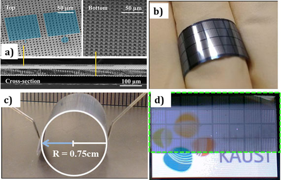 |
| (a) Scanning electron microscopic (SEM) images of top, crosssection, and bottom view of a released sample. The top view shows the capacitors’ geometries (blue), the bottom shows ALD-spacers regularity, and the cross-section shows thickness uniformity; (b) released sample wrapped around a finger, displaying great flexibility; (c) minimum bending radius before fracture; (d) semi-transparent sample covering portion of a LED screen with KAUST logo. (Reprinted with permission from American Institute of Physics) |
| "With the fabrication technique that we developed, we build devices following state-of-the-art CMOS compatible processes and then etch trenches through the silicon’s unused real estate in between devices followed by a vertical sidewall formation to protect the devices and the underlying silicon," Hussain explains the fabrication process to Nanowerk. "We then perform an isotropic silicon etching to remove the silicon from the inner portion of the substrate, forming caves which – when interconnecting with others – eventually release the top portion of the substrate so that the devices can be peeled off." |
| He points out that, unlike in MEMS processes where a sacrificial layer is removed to free the top layer which we term as silicon fabric, in their case no sacrificial layer is needed but rather they use a hard top mask to shield the top surface (where the devices are located) and a spacer-like protection technique to protect the holes integrity from the chemical effect of the subsequent releasing isotropic-etching step. |
| "The released silicon wafer – we have demonstrated up to 4” diameter silicon wafer – is mechanically flexible and optically transparent," says Hussain. "This process allows to maintain the same performance level required for high performance computation and it does not compromise ultra-high resolution lithographic demand for billions of transistor integration; multi-level interconnects for complex circuitry fabrication; and affordability." |
| In addition, the researchers have also tested that the remaining substrate is reusable after a chemical mechanical polishing (CMP). |
| "Although it is true that organic electronics can be fabricated using low-cost 'garage fabrication', the per-bit information/area cost is much lower in silicon chips," says Hussain. "Therefore, our work shows a pragmatic path to building such advanced devices on a flexible as well as transparent platform of silicon – the most common and friendly name in electronics." |
 By
Michael
Berger
– Michael is author of four books by the Royal Society of Chemistry:
Nano-Society: Pushing the Boundaries of Technology (2009),
Nanotechnology: The Future is Tiny (2016),
Nanoengineering: The Skills and Tools Making Technology Invisible (2019), and
Waste not! How Nanotechnologies Can Increase Efficiencies Throughout Society (2025)
Copyright ©
Nanowerk LLC
By
Michael
Berger
– Michael is author of four books by the Royal Society of Chemistry:
Nano-Society: Pushing the Boundaries of Technology (2009),
Nanotechnology: The Future is Tiny (2016),
Nanoengineering: The Skills and Tools Making Technology Invisible (2019), and
Waste not! How Nanotechnologies Can Increase Efficiencies Throughout Society (2025)
Copyright ©
Nanowerk LLC
|

Become a Spotlight guest author! Join our large and growing group of guest contributors. Have you just published a scientific paper or have other exciting developments to share with the nanotechnology community? Here is how to publish on nanowerk.com. |
