Showing Spotlights 25 - 32 of 338 in category All (newest first):
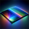 Recent breakthroughs integrate molybdenum disulfide transistor circuitry with large-area perovskite LEDs, promising unprecedented display quality with rapid response times and enhanced cost-efficiency.
Dec 13th, 2023
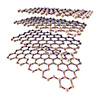 Super Holey Graphene enhances the already impressive properties of graphene, making it a significant breakthrough in materials science.
Dec 4th, 2023
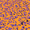
 A novel tunable stealth material design drawing inspiration from leaves can provide adjustable radar and infrared camouflage from a single lightweight structure, overcoming challenges that have impeded multifunctional stealth technologies for decades.
Nov 29th, 2023
 Synergistic multilevel graphene-MOF membrane excels in advanced water purification, efficiently filtering a wide range of contaminants.
Nov 16th, 2023
 Novel biomimetic reinforced graphene architecture overcomes mechanical fragility issues that previously hindered scalable fabrication of graphene membranes for selective transport.
Nov 14th, 2023
 Rresearchers report a new liquid templating strategy for engineering highly tunable, durable aerogels. The customizable gels showed improved emi shielding and record oil absorption.
Nov 3rd, 2023
 Researchers developed a method to assemble 2D nanosheets like MXene in 3D configurations using an infiltrated porous ceramic scaffold. This overcomes nanosheet restacking and may enable advances in energy, electronics, catalysis and more.
Oct 31st, 2023
 Researchers developed an ultra-thin, shape-changing speaker using advanced nanomaterials like MXene. It may allow seamlessly embedding speakers into clothing and objects.
Oct 20th, 2023
 Subscribe to our Nanotechnology Spotlight feed