| Nov 07, 2022 |
New quasiparticle discovered in moire patterns
(Nanowerk News) If you hold one wire mesh on top of another one and look through it, you'll see a larger pattern called a moiré pattern formed by the overlapping grids of the two meshes, which depends on their relative twisted angle. Scientists developing new materials are actively studying moiré patterns in overlapping atomically thin materials — they produce intriguing electronic phenomena that includes unconventional superconductivity and ferromagnetism.
|
|
Supercomputer simulations have helped scientists reveal in a bilayer moiré system a new species of an electronic phenomenon called an exciton, which is an electrically neutral quasiparticle, yet one that can carry energy and consists of an electron and electron ‘hole' that can be created for example by light impinging certain semiconductors and other materials.
|
|
The newly discovered excitons were produced by moiré patterns from two-dimensional sheets of exotic semiconductors called transition metal dichalcogenides, with the electron bound to the hole but separated from each other by a characteristic distance in the sheet. This was named an intralayer charge-transfer exciton and was a surprise to the scientists because such excitons do not exist in the individual sheets. The research can be used in the development of new optical sensors and communication technology such as optical fibers and lasers.
|
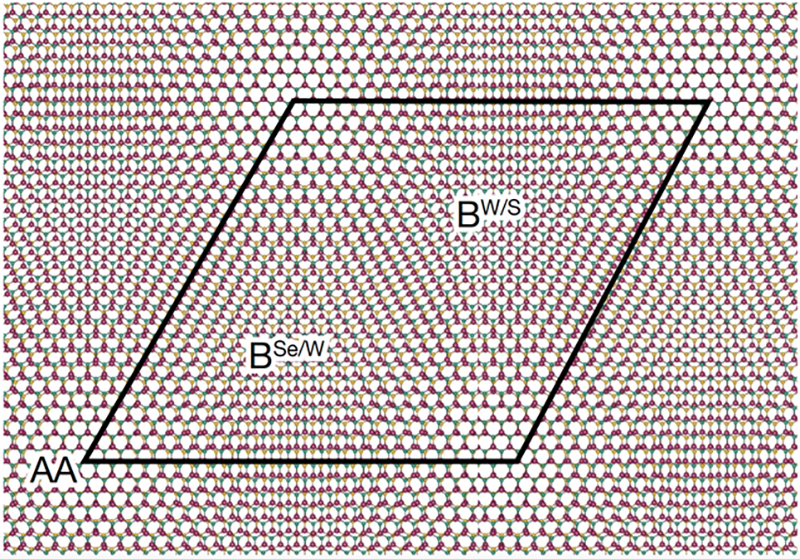 |
| Scientists have discovered a new kind of quasiparticle called an intralayer charge-transfer exciton, consisting of an electron and an electron hole separated in a characteristic distance, in a moiré superlattice formed by stacking one 2D layer of the material transition metal dichalcogenide on top of another with a slight twist. Rotationally aligned WSe2/WS2 heterostructure with the superlattice cell outlined in black and the high-symmetry positions labeled. (© Nature)
|
Novel exiton discovered
|
|
"In this work we discovered a novel exciton of unforeseen intralayer charge-transfer characteristics in a moiré superlattice formed by two atomically thin layers of transition metal dichalcogenide materials," said Steven G. Louie, a distinguished professor of physics at the University of California, Berkeley (UC Berkeley), and a senior faculty scientist at the Lawrence Berkeley National Laboratory (LBNL).
|
|
Louie is the corresponding author of research published in the journal Nature ("Intralayer charge-transfer moiré excitons in van der Waals superlattices"). In it, the scientists developed computer models that go beyond the conventional parameterized models that have been used to describe moiré systems and moiré excitons. Instead, they performed ab initio calculations that only start with the identity and initial position of the 3,903 atoms of the moiré superlattice unit cell.
|
First principles
|
|
"It is a powerful method to accurately predict material properties," Louie added, "because there's no empirical fitting involved."
|
|
In particular, to calculate the exciton states and the optical property of the moiré systems, they used the state-of-the-art GW plus Bethe–Salpeter equation (GW-BSE) approach, considered one of the most accurate approaches to predicting the optical properties of materials.
|
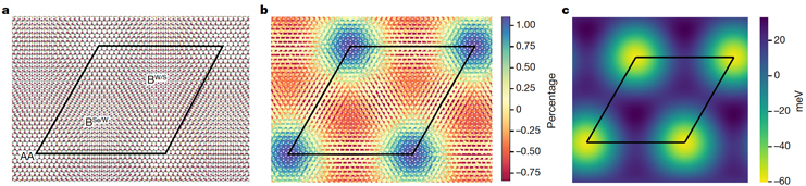 |
| Reconstruction of the moiré superlattice. (a) Moiré superlattice with unit cell outlined in black. (b) Strain distribution in the WSe2 layer as a result of structural reconstruction. (© Nature)
|
|
What's more, Louie and colleagues used their calculations to predict the different electronic and optical responses of the excitons in the system. They worked with experimental colleagues Emma C. Regan, Zuocheng Zhang and Professor Feng Wang at UC Berkeley. In a nutshell, Wang and colleagues shone light on the material and then analyzed the reflected light to see how the system responded to the impinging photons under different conditions.
|
|
Sure enough, they verified the theoretical predictions by finding distinct signatures of the intralayer charge-transfer exciton in their measurements.
|
|
"The GW-BSE method is very accurate, but it is also very computationally challenging," said study co-author Mit Naik, a postdoctoral researcher working with Professor Louie at UC Berkeley and LBNL.
|
|
The challenge in simulating an exciton is that it requires solving difficult six-dimensional integrals, numerous times, and the integrals are massive in the moiré superlattice because of the large size of the moiré unit cell – composed of many unit cells of the individual layers, 25x25 for one layer and 26x26 for the other.
|
|
Typical GW-BSE calculations are performed on systems of just up to a hundred atoms in the unit cell. Here, the authors needed calculations for a whooping 3,903 atoms. "Initially, it seemed almost impossible," Naik said.
|
|
Undaunted, the scientists hit on a new method that reduced the computational cost by a million times without loss of accuracy.
|
|
"We found a way to approximate each layer's two thousand atom integral as a sum over many three atom integrals, which were computationally much simpler to compute," Naik said.
|
|
The theoretical technique they developed, called the pristine unit-cell matrix projection (PUMP) method, can be generalized to study other material systems such as interlayer or hybrid moiré excitons in multi-layer moiré superlattices, shallow defects in materials, and more.
|
|
The Texas Advanced Computing Center (TACC) supported Steven Louie's first principles study of cutting-edge materials through a large resource allocation on TACC's Frontera supercomputer, the most powerful academic system in the U.S and funded by the National Science Foundation.
|
|
He also was awarded allocations on TACC's Stampede2 supercomputer made through the NSF-funded Advanced Cyberinfrastructure Coordination Ecosystem: Services & Support (ACCESS), formerly the Extreme Science and Engineering Discovery Environment (XSEDE).
|
|
In their bid to push the limit of the number of atoms in their calculations, the researchers initially faced some problems with running some of the large-scale moiré calculations on Frontera.
|
|
"We received support from the research associates at TACC, who helped us resolve these problems," Naik recalled.
|
|
For instance, they were unable to run the large-scale simulations of ground-state properties on Frontera using a standard density functional theory (DFT) package called Quantum Espresso, because of the instability created by a new version of the Intel compiler used to for the DFT package.
|
|
The TACC consulting team found a way around the problem by installing an older, more stable version of the compiler. "This allowed us to compute the electronic structure of the WSe2 moiré superlattice that went into this work," Naik said.
|
|
"Frontera and Stampede2 hardware efficiently catered to our requirements by providing state-of-the-art internode connectivity and sufficient memory on each node," Naik added.
|
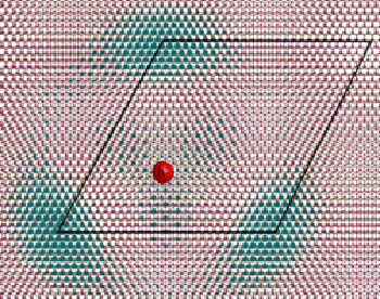 |
| Calculated electron density isosurface (4% of maximum) for a particular intralayer moiré exciton with the hole coordinates fixed at a point (red sphere), showing the spatial separation of electron density from the hole, or a charge-transfer character of the exciton. The solid lines enclose the moiré superlattice unit cell. (© Nature)
|
Science impact
|
|
"The intralayer charge-transfer exciton we discovered through this artificial stacking of two monolayers has revealed an extraordinarily strong interplay of the atomic structure and the type of exciton possible in the moiré systems," Louie said. "This is an important step in advancing the engineering of materials for desired properties."
|
|
That's because, once light creates charge-transfer excitons, they can be distorted or dissociated more easily with an external field or other perturbations than the standard Wannier-type excitons.
|
|
These considerations are important in many basic phenomena and potential applications, such as novel optical sensors and electro-optic modulation nanodevices. "That's what we're working on with our experimental colleagues right now," Louie said.
|
|
"Excitonic properties of materials form the basic principles behind many of the optical and optoelectronic devices and sensors that we encounter in our daily lives," said study co-author Felipe Jornada, an Assistant Professor in the Department of Materials Science and Engineering at Stanford University and a Principal Investigator at the SLAC National Accelerator Laboratory.
|
|
He gave the example of OLED TVs and displays, which use light emission from the recombination of excitons in organic semiconductors. Also, new smartwatches use advanced optical sensors to monitor the wearer's blood oxygen levels.
|
|
"Beyond existing devices, the transition metal dichalcogenides and heterostructures of these materials that we're working on are considered a promising material platform for post-silicon nanoscale optoelectronic devices. Moving forward, we believe that these are going to be a promising route towards novel sensors, displays, and technologies," Jornada said.
|

