| Apr 08, 2021 |
An inverse-designed metalens 3D-printed on an optical fiber tip |
| (Nanowerk Spotlight) Electronic devices have gotten much smaller and more efficient over the years but the design and underlying physics of today's optical lenses haven't changed much since antiquity. Consequently, conventional optical elements are bulky – much larger than the operating wavelength – and often require rigorous alignment. |
| A new generation of lenses – metalenses – is starting to replace bulky curved lenses with simple, flat surfaces that use nanostructures to focus light. These flat surfaces – metasurfaces – have enabled the design of diffraction-based flat devices to replicate the functionalities of conventional lenses with sub-wavelength or few-wavelength thicknesses. |
| These metasurface materials have led to the development of novel optical devices (holograms, gratings, axicons, polarization-selective devices) and might even put true holographic movies within grasp. |
| In new work reported in Nano Letters ("Inverse Design and 3D Printing of a Metalens on an Optical Fiber Tip for Direct Laser Lithography"), researchers at Northwestern University have now successfully designed and experimentally demonstrated an inverse-designed metalens to operate at a near-infrared wavelength. |
| "Our study highlights an alternative way of designing optical elements by considering the inverse problem without any prior knowledge of the structures," Koray Aydin, an associate professor at Northwestern's McCormick School of Engineering, explains to Nanowerk. "By implementing the inverse-design method, we have designed a high numerical aperture metalens compatible to be printed on a fiber tip." |
| Aydin and his team worked in collaboration with Prof. Sridhar Krishnaswamy’s group at Northwestern Mechanical Engineering. |
| Unlike the conventional way of designing optical elements – where one starts with a well-known studied structure – the inverse-design method allows for arbitrary initial guesses for an optimal design. This is achieved by setting a hard constraint on the objective of the design and searching for optimal design inversely. |
| "Combining both inverse-design method and two-photo polymerization opens a new alternative for fabricating complicated optical structures that are rather difficult to achieve using conventional microfabrication techniques," Aydin points out. |
 |
| Figure 1. (a) Problem definition of the inverse design. The incoming plane wave from the left is transformed into a spherical wavefront as it propagates to the right. (b) Objective-first inverse design optimized lens structure in 2D. (c) Three-dimensional lens obtained by taking the rotational symmetry of the 2D optimized lens. (d) Scanning electron microscope image of a sliced fabricated lens for characterization purposes. The scale bar shown is 2 µm. (Reprinted with permission by American Chemical Society) (click on image to enlarge) |
| "The optimized design is an effectively symmetric two-dimensional lens," Aydin notes. "To obtain a fully three-dimensional lens, we took advantage of the rotational symmetry of the 2D lens. We rotated the lens around its middle axis to create the 3D lens," (as shown in Figure 1c above). |
| Experimentally, Aydin and his team fabricated the metalens using a two-photon polymerization system, commonly known as 3D nanoprinter, which is capable of printing structures on the order of 100 nm. |
| Also, as shown in this study, the fiber tip metalens facilitates the printing of structures on non-conventional surfaces, which is not easily accessible by bulky commercial direct laser printers. |
| To demonstrate the effectiveness of their approach, the team built a homemade direct laser printing system using the fabricated metalens on a fiber tip. They show that their miniaturized optical element performs similar or better than its bulky counterparts. |
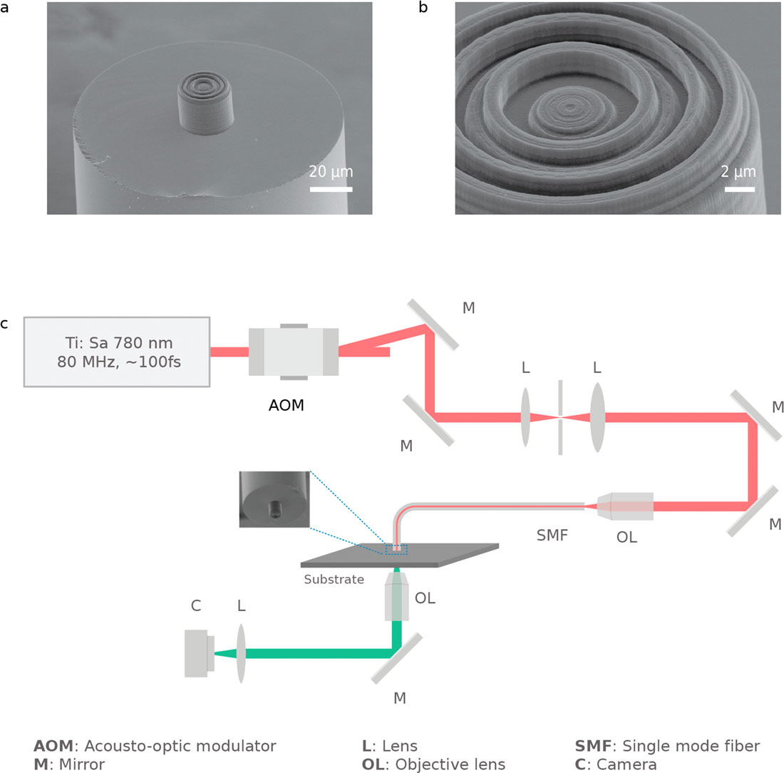 |
| Figure 2. (a) Scanning electron microscopy image of the fabricated fiber tip lens on top of a single mode fiber (SMF). (b) Enlarged view of the fabricated fiber-tip lens. (c) Schematic of the homemade two photon polymerization setup, employing the fabricated fiber-tip lens as the objective lens. (Reprinted with permission by American Chemical Society) (click on image to enlarge) |
| "It is also important to note that our approach is not limited to a metalens as shown in this particular study," Aydin says. "Our strategy can also be applied as a simpler and cost-effective alternative to various other optical applications such as imaging, optical endoscopes, optical nanoparticle trapping, etc." |
| The immediate possible application of this work is the ability to print and create structures on surfaces that are otherwise difficult to achieve using conventional direct laser printing systems. |
| "The current implementation of inverse design still involves a computationally relatively expensive Maxwell equation solver, which limits the extent of the design domain of the optical structures," Aydin notes. "With emerging machine learning applications in nanophotonics, more efficient solvers might be realized and thus expand the possibilities of optical design." |
| "On a more practical note, one particular challenge is to achieve robust and high-throughput fabrications using a two-photon polymerization setup," he concludes. "Currently, it is more suitable for rapid prototyping where easy and quick to realize optical elements are needed." |
 By
Michael
Berger
– Michael is author of four books by the Royal Society of Chemistry:
Nano-Society: Pushing the Boundaries of Technology (2009),
Nanotechnology: The Future is Tiny (2016),
Nanoengineering: The Skills and Tools Making Technology Invisible (2019), and
Waste not! How Nanotechnologies Can Increase Efficiencies Throughout Society (2025)
Copyright ©
Nanowerk LLC
By
Michael
Berger
– Michael is author of four books by the Royal Society of Chemistry:
Nano-Society: Pushing the Boundaries of Technology (2009),
Nanotechnology: The Future is Tiny (2016),
Nanoengineering: The Skills and Tools Making Technology Invisible (2019), and
Waste not! How Nanotechnologies Can Increase Efficiencies Throughout Society (2025)
Copyright ©
Nanowerk LLC
|

Become a Spotlight guest author! Join our large and growing group of guest contributors. Have you just published a scientific paper or have other exciting developments to share with the nanotechnology community? Here is how to publish on nanowerk.com. |
