| Posted: Feb 27, 2007 | |
Gutenberg + nanotechnology = printable electronics |
|
| (Nanowerk Spotlight) Nanoelectronics devices often are made by integrating dissimilar classes of semiconductors and various other disparate materials into one heterogeneous single system. The two primary modes of combining these materials – mechanical bonding and epitaxial growth processes - place stringent requirements on the ultimate scale or constituent materials of circuits. | |
| With mechanical bonding, there is a limited ability to scale to large areas (i.e., larger than the wafers) or to more than a few stacking layers; incompatibility with unusual materials (such as nanostructured materials) and/or low-temperature materials and substrates; challenging fabrication and alignment for the through-wafer electrical interconnects; demanding requirements for planar bonding surfaces; and bowing and cracking that can occur from mechanical strains generated by differential thermal expansion and contraction of disparate materials. | |
| Epitaxy avoids some of these problems but places severe restrictions on the quality and type of materials that can be grown. Using a process akin to the printing press, researchers have managed to bypass the need for epitaxial growth or wafer bonding to integrate wide ranging classes of dissimilar semiconducting nanomaterials onto substrates for the purpose of constructing heterogeneous, three dimensional electronics. | |
| Printed semiconductor nanomaterials provide new approaches to 3D heterogeneously integrated systems that could be important in various fields of applications such as microfluidic devices with integrated electronics, chemical and biological sensor systems that incorporate unusual materials with conventional silicon-based electronics, and photonic and optoelectronic systems that combine light emitters and detectors of compound semiconductor with silicon drive electronics or micro electromechanical structures. | |
| Furthermore, the compatibility of this approach with thin, lightweight plastic substrates may create additional opportunities for devices that have unusual form factors or mechanical flexibility as key features. | |
 |
|
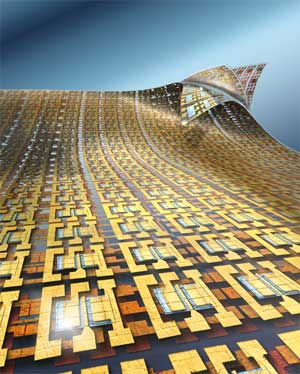
| Illustration based on confocal images of actual three layer stacks of transistors that use single crystal ribbons of silicon for the semiconductor and a thin sheet of polyimide for the substrate. (Image: Rogers Research Group) | |
| "Our approach, the combined use of semiconductor nanomaterials and printing techniques, enables high quality electronics to be formed on diverse substrates, including nonplanar surfaces and thin plastic sheets" John A. Rogers tells Nanowerk. "These capabilities, in particular the ability to use any mixture of component materials, all lie well outside of the range of things that can be achieved with conventional wafer based approaches to electronics." | |
| Rogers, a professor of chemistry, materials science and engineering at the University of Illinois at Urbana-Champaign, and his research group are trying to develop approaches that enable "high performance electronics anywhere", i.e. they would like to extend semiconductor device technology to substrates other than the semiconductor wafer. | |
| "Our goal is to invent methods that can allow interesting applications which cannot be addressed with conventional technologies, such as flexible displays, large area solar cells, conformable X-ray imagers, distributed structural and personal health monitors, curved surface imagers as electronic eyes, etc" says Rogers. "Our belief is that inorganic semiconductor nanomaterials, delivered to a target device substrate using printing techniques, forms an attractive way to achieve devices of these types." | |
| The recent results by Roger's group show how dissimilar single-crystal inorganic semiconductors (such as micro- and nanoscale wires and ribbons of GaN, Si, and GaAs) can be combined with one another and also with other classes of nanomaterials (such as single-walled carbon nanotubes - SWCNTs) with the use of a scalable and deterministic printing method to yield complex, heterogeneously integrated electronic systems in 2D or 3D layouts. | |
| Specifically, the nanoscale semiconductor components are first fabricated, each on their own source substrate, through standard lithographic procedures, with ohmic contacts formed by doping and annealing. These components are then lifted from the source substrate by gentle van der Waals adhesion with an "inking pad" made of polydimethylsiloxane, and then "stamped" onto a device substrate such as a sheet of polyimide. | |
| After some additional processing – including deposition and patterning of gate dielectrics, electrodes, and interconnects – the transfer printing and device fabrication steps can be repeated, beginning with spin-coating a new prepolymer interlayer on top of the previously completed circuit level. | |
| Rogers points out that this fabrication approach has several important features: | |
| First, all of the processing on the device substrate occurs at low temperatures, thereby avoiding differential thermal expansion and shrinkage effects that can result in unwanted deformations in multilayer stacked systems. This operation also enables the use of low-temperature plastic substrates and interlayer materials, and it helps to ensure that underlying circuit layers are not thermally degraded by the processing of overlying devices. | |
| Second, the method is applicable to broad classes of semiconductor nanomaterials, including emerging materials such as SWNTs. | |
| Third, the soft stamps enable nondestructive contacts with underlying device layers; these stamps, together with the ultrathin semiconductor materials, can also tolerate surfaces that have some topography. | |
| Fourth, the ultrathin device geometries and interlayers allow easy formation of layer-to-layer electrical interconnects by direct metallization over the device structure. These features overcome many of the disadvantages of conventional approaches. | |
| The researchers demonstrated the capabilities of their printing process by fabricating ultrathin multilayer stacks of high-performance metal oxide semiconductor field-effect transistors (MOSFETs), high electron mobility transistors (HEMTs), thin-film transistors (TFTs), photodiodes, and other components that are integrated into device arrays, logic gates, and actively addressable photodetectors on rigid inorganic and flexible plastic substrates. | |
| "We are now working to make these kinds of approaches realistic methods for manufacturing" says Rogers. "We focus on (1) the development of tooling to automate the process, and (2) demonstrator devices, i.e. electronic eye imagers, large area solar cells, and flexible displays), that can illustrate the utility of these approaches." | |
| These findings have been published in a recent paper in the December 15, 2006 issue of Science ("Heterogeneous Three-Dimensional Electronics by Use of Printed Semiconductor Nanomaterials"). | |
 By
Michael
Berger
– Michael is author of three books by the Royal Society of Chemistry:
Nano-Society: Pushing the Boundaries of Technology,
Nanotechnology: The Future is Tiny, and
Nanoengineering: The Skills and Tools Making Technology Invisible
Copyright ©
Nanowerk LLC
By
Michael
Berger
– Michael is author of three books by the Royal Society of Chemistry:
Nano-Society: Pushing the Boundaries of Technology,
Nanotechnology: The Future is Tiny, and
Nanoengineering: The Skills and Tools Making Technology Invisible
Copyright ©
Nanowerk LLC
|
Become a Spotlight guest author! Join our large and growing group of guest contributors. Have you just published a scientific paper or have other exciting developments to share with the nanotechnology community? Here is how to publish on nanowerk.com.