| Posted: Nov 09, 2010 | |
The rise of white graphene |
|
| (Nanowerk Spotlight) Graphene nanoribbons – atomically-thin strips of graphene that are just a few nanometers wide – are considered to be excellent candidates for future electronics applications as their properties can be adjusted through width and edge shape (see: "Nanoribbons for graphene transistors for tomorrow's nanoelectronics"). | |
| Along with graphene, boron nitride nanoribbons have attracted more and more fundamental research interest. For instance, researchers have found that magnetism could be induced in such ribbons by the replacement of B or N with Be, B, C, N, O, Al, and Si, or with vacancy defects (see: "Magnetism of C Adatoms on BN Nanostructures: Implications for Functional Nanodevices"). They also found that the ribbons could have a narrowed band gap and improved electrical conductivity tuned by a transverse electric field or special edge structure (see for instance: "Energy Gaps and Stark Effect in Boron Nitride Nanoribbons"). These findings promise a bright future in in optoelectronics and spintronics for atomically thin boron nitride nanoribbons. | |
| However, a major challenge in providing experimental evidence is that the preparation of atomically thin boron nitride nanoribbons is very difficult. | |
| "Previous experiments and design theories suggest that the intercalation of molecules into a boron nitride interlayer space is much more difficult compared to graphite" Haibo Zeng, a research scientist at the International Center for Materials Nanoarchitectonics (MANA) in Japan, explains to Nanowerk. "Furthermore, the interlayer interactions of boron nitride layers are stronger than those in graphite. This creates significant difficulties in standard chemical exfoliation and mechanical cleaving of boron nitride crystals into nanoribbons." | |
 |
|
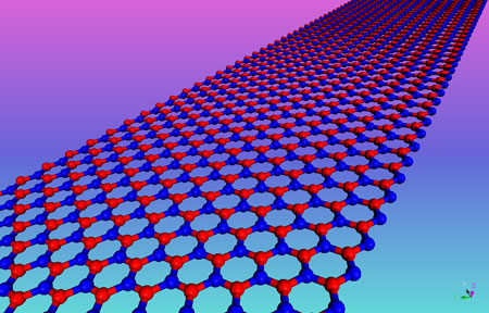
| Atomic structural motif of a zigzag boron nitride nanoribbon. (Image: Haibo Zeng, MANA) | |
| In new work that represents an important step in bridging theoretical predictions and experimental realization of atomically thin boron nitride nanoribbons, Zeng and coworkers (from National Institute for Materials Science (NIMS) in Japan and Nanjing University of Aeronautics and Astronautics (NUAA) in China) demonstrate the successful fabrication of 'white graphene' nanoribbons – made of thermally and chemically stable atomic layers of hexagonal boron nitride (h-BN) – by unwrapping multiwalled boron nitride nanotubes under delicate argon plasma etching. They show that the insulator-semiconductor electrical transition takes place during this processing and that this typically electrically insulating compound becomes a semiconductor when it is in ribbon morphology. | |
| The team has reported their findings in the October 28, 2010 online issue of Nano Letters (""White Graphenes": Boron Nitride Nanoribbons via Boron Nitride Nanotube Unwrapping"). | |
| h-BN is a layered material analogous to graphite – the hexagonal honeycomb-like layers made of alternating B and N atoms are stacked so that each B3N3 hexagons is placed above and below N3B3 hexagons. Similarly to carbon nanotubes, there exist boron nitride nanotubes, however, compared with hardly predictable electrical performance of carbon nanotubes that strongly depends on the graphene sheet wrapping angle and other structural parameters, boron nitride nanotubes are insulating with a bandgap of ∼5.5 eV that is nearly independent of tube diameter, chirality, and number of tube walls. | |
| Zeng explains that, in their fabrication process, they first embedded the initial boron nitride multiwalled nanotubes in a polymer film with one tube wall side exposed, and then the plasma etching was implemented to consecutively unzip, unwrap and exfoliate the tube walls. | |
| This process led to the formation of atomically thin boron nitride nanoribbons. Although there have been a few reports on the fabrication of boron nitride sheets, the NIMS and NUAA researchers have made a significant step further: this is the first report on the controllable production of atomically thin boron nitride nanoribbons. The nanoribbon widths are determined by the starting nanotube shell diameters and plasma parameters. The obtained boron nitride nanoribbons can be as narrow as 10 nm and as thin as one atomic monolayer. | |
| "With regard to 2-dimensional (2D) crystals, the nanoribbons are quite different from the larger sheets with several hundred nanometers dimensions" says Zeng. "The key point is that the electronic and spin states of the 2D crystal edges are completely different from the other parts. While this has been well demonstrated in graphene nanoribbons, the lack of practical fabrication techniques for boron nitride nanoribbons has posed a persistent challenge in advancing to a practical device level and deeper understanding on the rich physics involved." | |
 |
|
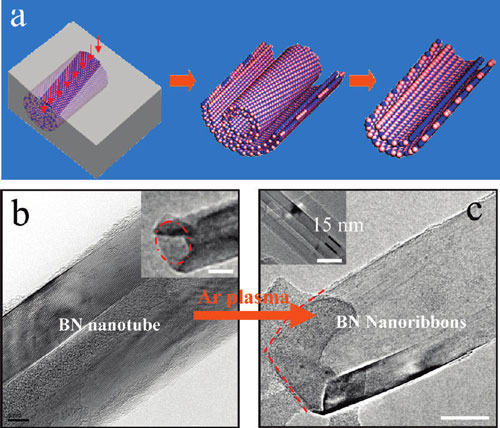
| Unwrapping multiwalled boron nitride nanotubes. (a) Schematic of the unwrapping processes induced by plasma etching, the stepwise opening/unzipping, removing and exfoliating of tube walls to form "white graphene" nanoribbons is sketched. (b,c) Typical TEM images of products before and after etching, demonstrating the morphology transition. The inset in b reveals the open and nearly circular end of the initial tube, and the inset in c shows four formed ribbons; the scale bars are 20 nm. (Reprinted with permission from American Chemical Society) | |
| The NIMS team found that the nanoribbons had preferred to possess zigzag edges and had been prone to numerous surface vacancies. This kind of edge structures is very important and induces abundant properties. | |
| "The observed atomic structures could be caused by the specific plasma-induced processing and currently it is not fully clear whether they are intrinsic for boron nitride nanoribbons" says Dmitri Golberg, a principal investigator at MANA. "This needs to be compared with boron nitride nanoribbons produced by other methods." | |
| A joint NIMS and NUAA team is now conducting theoretical work on the observed electronic transition. "The observed electronic transition from an insulator to a semiconductor during the formation of boron nitride nanoribbons is very interesting and should greatly expand this unique material's application in electronic and optoelectronic devices," Wanlin Guo, a Professor at NUAA, points out. | |
| The improved electrical conductivity is induced by the shallow acceptor-like doping effects of experimentally proven zigzag ribbon edges and surface vacancies. | |
| "Especially when considering the much better thermal and chemical stability of boron nitride compared to graphite, these structures could be particularly valuable in high temperature and hazardous environments" says Guo. | |
| According to the researchers, another important potential application of boron nitride nanoribbons is their utilization as epitaxial substrates and/or gate layers for graphene devices due to their suitable dielectric constant and a perfect match in lattice parameters and atomic structures between carbon and boron nitride phases. | |
| Currently, white graphenes, i.e. BN 2D crystals, have become a rapidly rising field, but it is still in its infancy period. It is calling researchers in physics, chemistry, and materials fields to fabricate better samples with a high ratio of monolayers and at larger yields to make it possible a full range exploration of novel properties and new performances related to them. | |
 By
Michael
Berger
– Michael is author of three books by the Royal Society of Chemistry:
Nano-Society: Pushing the Boundaries of Technology,
Nanotechnology: The Future is Tiny, and
Nanoengineering: The Skills and Tools Making Technology Invisible
Copyright ©
Nanowerk LLC
By
Michael
Berger
– Michael is author of three books by the Royal Society of Chemistry:
Nano-Society: Pushing the Boundaries of Technology,
Nanotechnology: The Future is Tiny, and
Nanoengineering: The Skills and Tools Making Technology Invisible
Copyright ©
Nanowerk LLC
|
|
| Reference: Zeng, H., Zhi, C., Zhang, Z., Wei, X., Wang, X., Guo, W., Bando, Y., & Golberg, D. (2010). "White Graphenes": Boron Nitride Nanoribbons via Boron Nitride Nanotube Unwrapping Nano Letters DOI: 10.1021/nl103251m | |
|
Become a Spotlight guest author! Join our large and growing group of guest contributors. Have you just published a scientific paper or have other exciting developments to share with the nanotechnology community? Here is how to publish on nanowerk.com. |
|