| Posted: Feb 03, 2011 | |
Conformal printing of 3D electrically small antennas |
|
| (Nanowerk Spotlight) Electrically small antennas (ESA) find use in a wide variety of communications platforms – e.g. mobile phones an other handheld devices, RFID, aerospace and defense systems – but their construction requires advances in printing as well as a robust antenna design so that their operating frequency, size, and system impedance could be easily varied. | |
| In order for an antenna to be 'electrically small', the largest dimension of the antenna should be no more than one-tenth of a wavelength. For instance, a 9 square-centimeter RFID tag will have an antenna that is considered electrically small at any frequency below about ∼1.1 GHz. | |
| Especially RFID (radio-frequency identification) tags have received a lot of attention recently with regard to developing electronic toll collection, payment by mobile phone, e-passports, product tracking etc. To date, RFID antennas have been produced by screen-printing or inkjet printing in simple motifs, such as dipoles and loops. A significant disadvantage of these fabrication techniques is that they are limited in both spatial resolution and dimensionality – yielding planar antennas that occupy a large area relative to the achieved performance. | |
| Researchers have now demonstrated the conformal printing of electrically small antennas on spherical shapes with a key performance metric (radiation quality factor or Q) that very closely approaches the fundamental limit dictated by physics (Chu limit; see: "Physical limitations of omnidirectional antennas"). | |
| "Our fundamental design approach enables specification of both operating frequency and size, while achieving near-optimal bandwidth at several frequencies of interest for wireless communications," Jennifer A. Lewis tells Nanowerk. "The ability to conformally print antennas that are compact and encapsulated within their support substrate further enhances their mechanical robustness. More broadly, conformal printing of conducting features may enable several applications, including flexible, implantable and wearable antennas, electronics, and sensors." | |
| Lewis, the Hans Thurnauer Professor of Materials Science and Engineering, Willett Faculty Scholar of Engineering, and Director, F. Seitz Materials Research Laboratory at the University of Illinois at Urbana-Champaign (UI), together with Jennifer T. Bernhard, a professor in the Department of Electrical and Computer Engineering at UI, and their groups have published their findings in the January 19, 2011 online edition of Advanced Materials ("Conformal Printing of Electrically Small Antennas on Three-Dimensional Surfaces"). | |
| "The problem of minimizing the Q of an electrically small antenna is a long-standing one in the antenna community," explains Bernhard. "We have demonstrated a highly versatile design for a single-mode antenna that minimizes Q for the required maximum dimension, which is realizable in a hemispherical motif." | |
 |
|
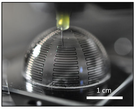
| Optical image of an antenna during the printing process of meander lines made of silver nanoparticle ink. (Image: Lewis Group, University of Illinois at Urbana-Champaign) | |
| The 3D ESAs developed by the UI team are fabricated by conformal printing of metallic inks onto convex and concave hemispherical surfaces in the form of conductive meander lines (see image above). Their bandwidth approaches the fundamental limit for their size, offering nearly an order of magnitude improvement over rudimentary monopole antenna designs. | |
| "With our approach, antennas can be rapidly adapted to new specifications, including other operating frequencies, device sizes, or encapsulated designs that offer enhanced mechanical robustness" says Lewis. "Non-spherical ESAs can be designed and printed using a similar approach to enable integration of low Q antennas on the inside of a cell phone case, for example." | |
| The 3D antennas are fabricated by conformal printing of a concentrated silver nanoparticle ink in a digitally programmed meander line pattern onto either the exterior (convex) or interior (concave) surface of a hollow glass hemisphere (if printed on the inside, the hollow glass hemisphere serves as a protective barrier, allowing the device to be easily handled and mounted). The researchers point out that, unlike planar substrates, the surface normal is constantly changing on curvilinear surfaces, which presents added fabrication challenges. | |
| After printing and annealing at 550 °C, the patterned meander lines exhibit an electrical resistivity of ∼5 ? 10-6 Ω?cm. The antenna's operating frequency is determined primarily by the printed conductor cross-section and the spacing (or pitch) between meander lines within each arm. | |
| The team is currently designing and printing new antennas with multiple radiating modes to further enhance antenna performance. | |
| The video below shows a shows a representative antenna being patterned on the outer surface of the glass hemisphere: | |
 By
Michael
Berger
– Michael is author of three books by the Royal Society of Chemistry:
Nano-Society: Pushing the Boundaries of Technology,
Nanotechnology: The Future is Tiny, and
Nanoengineering: The Skills and Tools Making Technology Invisible
Copyright ©
Nanowerk LLC
By
Michael
Berger
– Michael is author of three books by the Royal Society of Chemistry:
Nano-Society: Pushing the Boundaries of Technology,
Nanotechnology: The Future is Tiny, and
Nanoengineering: The Skills and Tools Making Technology Invisible
Copyright ©
Nanowerk LLC
|
|
|
Become a Spotlight guest author! Join our large and growing group of guest contributors. Have you just published a scientific paper or have other exciting developments to share with the nanotechnology community? Here is how to publish on nanowerk.com. |
|