| Posted: Aug 08, 2007 | |
Nanotechnology researchers go ballistic over graphene |
|
| (Nanowerk Spotlight) Carbon comes in many different forms, from the graphite found in pencils to the world's most expensive diamonds. In 1980, we knew of only three basic forms of carbon, namely diamond, graphite, and amorphous carbon. Then, fullerenes and carbon nanotubes were discovered and all of a sudden that was where nanotechnology researchers wanted to be. Recently, though, there has been quite a buzz about graphene. Discovered only in 2004, graphene is a flat one-atom thick sheet of carbon. | |
| Existing forms of carbon basically consist of sheets of graphene, either bonded on top of each other to form a solid material like the graphite in your pencil, or rolled up into carbon nanotubes (think of a single-walled carbon nanotube as a graphene cylinder) or folded into fullerenes. Physicists had long considered a free-standing form of planar graphene impossible; the conventional wisdom was that such a sheet always would roll up. Initially using such high-tech gadgets like pencils and sticky tape to strip chunks of graphite down to layers just one atom thick, the process has now been refined to involve more expensive instruments such as electron beam and atomic force microscopes. | |
| Despite being isolated only three years ago, graphene has already appeared in hundreds of papers. The reason scientists are so excited is that two-dimensional crystals (it's called 2D because it extends in only two dimensions - length and width; as the material is only one atom thick, the third dimension, height, is considered to be zero) open up a whole new class of materials with novel electronic, optical and mechanical properties. | |
 |
|
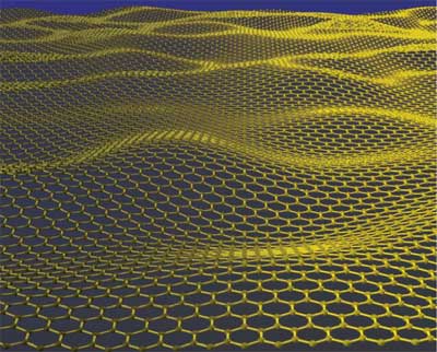
| Mother of all graphitic forms. Graphene is a 2D building material for carbon materials of all other dimensionalities. It can be wrapped up into 0D buckyballs, rolled into 1D nanotubes or stacked into 3D graphite. (Artistic impression of a corrugated graphene sheet: Jannik Meyer) | |
| "Owing to its unusual electronic spectrum, graphene has led to the emergence of a new paradigm of ‘relativistic’ condensed-matter physics, where quantum relativistic phenomena, some of which are unobservable in high-energy physics, can now be mimicked and tested in table-top experiments" Dr. Kostya Novoselov explains to Nanowerk. "More generally, graphene represents a conceptually new class of materials that are only one atom thick, and, on this basis, offers new inroads into low-dimensional physics that has never ceased to surprise and continues to provide a fertile ground for applications." | |
| Novoselov, The Royal Society Research Fellow, and a member of the Mesoscopic Physics Group at the University of Manchester, is one of the original team, led by Professor Andre Geim, that discovered graphene in 2004. In a recent progress article in Nature Materials ("The rise of graphene") Novoselov and Geim report on the current knowledge, ongoing efforts and expectation regarding graphene research. | |
| Experiments with graphene have revealed some fascinating phenomena that excite researchers working towards molecular electronics. Geim's team found that graphene remains capable of conducting electricity even at the limit of nominally zero carrier concentration because the electrons don't seem to slow down or localize. | |
| Novoselov says that the electrons moving around carbon atoms interact with the periodic potential of graphene’s honeycomb lattice, which gives rise to new quasiparticles that have lost their mass, or 'rest mass' (so-called massless Dirac fermions). That means that graphene never stops conducting. It was also found that they travel far faster than electrons in other semiconductors. | |
| In the ultimate nanoscale transistor – dubbed a ballistic transistor – the electrons avoid collisions, i.e. there is a virtually unimpeded flow of current. Ballistic conduction would enable incredibly fast switching devices. Graphene has the potential to enable ballistic transistors at room temperature. | |
| Already, efforts to develop graphene electronics are underway. A first report on confined geometries in graphene (graphene quantum dots) was done by Geims group in their above-mentioned review. At the Rensselaer Polytechnic Institute they are working on graphene nanoribbons. These ribbons have also been demonstrated by IBM and the Kim group at Columbia University. At Delft's Kavli Institute for Nanoscience they attach graphene to superconductors to get a a bipolar transistor for superconducting currents. | |
| "Whichever approach prevails" says Novoselov, "there are two immediate challenges: First, despite the recent progress in epitaxial growth of graphene, high-quality wafers suitable for industrial applications still remain to be demonstrated. Second, individual features in graphene devices need to be controlled accurately enough to provide sufficient reproducibility in their properties. | |
| "The latter is exactly the same challenge that the silicon technology has been dealing with successfully. For the time being, to make proof-of-principle nanometer-size devices, one can use electrochemical etching of graphene by scanning-probe nanolithography." | |
 |
|
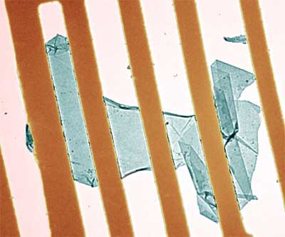
| Bright-field TEM image of a suspended graphene membrane. Its central part (bluish) is monolayer graphene. Electron diffraction images from different areas of the flake show that it is a single crystal without domains. Note scrolled top and bottom edges and a strongly folded region on the right. The typical distance between the golden bars is 500 nm. (Image: Jannik Meyer) | |
| Despite all the excitement, don't expect 'graphenium' microprocessors for at least another 20 years. Just look at carbon nanotubes. First observed in 1991, they have created tremendous excitement (and hype). But today, 16 years later, there are no commercial CNT-based breakthrough products on the market – although they supposedly make your golf balls go straighter (a breakthrough for some golfers at least). | |
| In the meantime, other graphene-based applications might come of age. Besides its electronic properties, graphene is also researched for its mechanical, thermal and optical properties. Already, existing graphene samples grown on silicon carbide substrate are of sufficient quality to be used for gas sensors. At Northwestern they work on graphene oxide paper and at Cornell they are building graphene resonators. Novoselov and Geim themselves have just reported a few days ago that graphene based sensors could sniff out dangerous molecules. Max Planck scientists, who work with Geim and Novoselov, are also interested in graphene sheets as membranes for biomolecular sensors. This idea to use graphene as a substrate to study biomolecules originated at the University of Zurich and there currently is a joint project – Structural Information of Biological Molecules at Atomic Resolution (SIBMAR) – where graphene could play a role. | |
| "The most immediate application for graphene is probably its use in composite materials" says Geim. "It would allow conductive plastics at less than one volume percent filling, which in combination with low production costs makes graphene-based composite materials attractive for a variety of uses. However, it seems doubtful that such composites can match the mechanical strength of their nanotube counterparts because of much stronger entanglement in the latter case." | |
| Another enticing possibility mentioned by Geim is the use of graphene powder in electric batteries that are already one of the main markets for graphite. "An ultimately large surface-to-volume ratio and high conductivity provided by graphene powder can lead to improvements in the efficiency of batteries, taking over from the carbon nanofibers used in modern batteries. Carbon nanotubes have also been considered for this application but graphene powder has an important advantage of being cheap to produce." | |
| Novoselov notes that It has been just over two years since graphene was first reported, and despite remarkably rapid progress, only the very tip of the iceberg has been uncovered so far. "Because of the short timescale, most experimental groups working now on graphene have not published even a single paper on the subject, which has been a truly frustrating experience for theorists. What has become clear, though, is that graphene is not a fleeting fashion but is here to stay, bringing up both more exciting physics, and perhaps even wideranging applications." | |
 By
Michael
Berger
– Michael is author of three books by the Royal Society of Chemistry:
Nano-Society: Pushing the Boundaries of Technology,
Nanotechnology: The Future is Tiny, and
Nanoengineering: The Skills and Tools Making Technology Invisible
Copyright ©
Nanowerk LLC
By
Michael
Berger
– Michael is author of three books by the Royal Society of Chemistry:
Nano-Society: Pushing the Boundaries of Technology,
Nanotechnology: The Future is Tiny, and
Nanoengineering: The Skills and Tools Making Technology Invisible
Copyright ©
Nanowerk LLC
|
Become a Spotlight guest author! Join our large and growing group of guest contributors. Have you just published a scientific paper or have other exciting developments to share with the nanotechnology community? Here is how to publish on nanowerk.com.