| Posted: Jul 10, 2014 | |
Self-assembly machines - a vision for the future of manufacturing |
|
| (Nanowerk Spotlight) Industrial production processes, by and large, rely on robotic assembly lines that place, package, and connect a variety of disparate components. While the manufacturing world is dominated by robots, there are applications where the established processes of serial 'pick and place' and manipulation of single objects reach scaling limits in terms of throughput, alignment precision, and the minimal component dimension they can handle effectively. | |
| By contrast, the emerging methods of engineered self-assembly are massively parallel and have the potential to overcome these scaling limitations. | |
| "So far researchers have focused on small area proof-of-concept demonstrations testing new self-assembly concepts – for example testing a different driving force, agitation, or component handling mechanism – inside a small container to define the environment where self-assembly takes place," Heiko Jacobs, a professor at Technische Universität Ilmenau and Chair of the university's Nanotechnology Group, tells Nanowerk. "Over the past 10 years, tremendous knowledge has been gained. However for many observers it leaves out the proof that any of the processes can be scaled to enable high volume production of real devices and products as promised at the outset." | |
| "Personally, I am convinced that this is possible and we are now at a stage where we have gained sufficient experience that will allow us to put the knowledge together to begin building 'self-assembly machines' which provides a deep motivation to go forward," he continues. | |
| In a paper in the June 27, 2014 online edition of Advanced Materials ("A First Implementation of an Automated Reel-to-Reel Fluidic Self-Assembly Machine"), Jacobs's team together with researchers from the University of Minnesota, describe the first example of a device to assemble and distribute LEDs over large areas for solid state lighting applications. | |
| It provides the blueprints and operational parameters of a reel-to-reel (RTR) fluidic self-assembly platform to assemble and electrically connect semiconductor chips with a yield clearly exceeding a 99% benchmark set by robotic pick and place machines. | |
 |
|
| Automated RTR fluidic self-assembly scheme. (A) Overview depicting (i) component dispensing on the basis of liquid flow and gravity which transports the components to empty self-assembly sites (receptors) on a continuously advancing web, (ii) where the components attach at predetermined locations on the basis of surface tension directed self-assembly, and (iii) where recycling of access components is achieved on the basis of gravity at the turning point of the web before they are transported upward on the basis of a fluid drag inside a sufficiently small diameter channel. Mechanical up and down motion of the web is used to induce liquid flow and shear forces to dispense and agitate the components as well as to aid in the removal of access component in the region of the upside-down oriented web. (B) Schematic depicting the details of surface tension directed self-assembly using molten-solder-bump-based receptors to capture and connect to the metal contacts on the chips. (C) A jet pump based principle is used to achieve recirculation of the chips without passing the components through a mechanical pump where they would get damaged. A preferred location of the jet pump is at the bottom of the slanted funnel where access components arrive on the basis of gravity to be picked up by a high velocity directional jet. (Reprinted with permission by Wiley-VCH Verlag) (click on image to enlarge) | |
| This machine is based on surface-tension-directed self-assembly. As the team points out, their assembly process is no longer a discontinuous small-batch hand-operated process but resembles an automated machine like process involving a conveyer belt and a RTR type assembly approach with automated agitation. | |
| The researchers' current design achieves 15,000 chips per hour using a 2.5 cm wide assembly region. Jacobs notes that scaling to 150,000 chips per hour would be possible using a 25 cm wide web, which would be a factor of 20 better than one of the faster chip pick-and-place machines in use today in the semiconductor industry. | |
| "In principle, scaling to any throughput should be possible considering the parallel nature of self-assembly and the fact that there is no requirement for any pick and place operations," he says. "This means that it is fairly straight forward to scale this technology to any desired assembly rate by increasing the substrate width and number of nozzles." | |
| Under optimized operational conditions, the group achieved an assembly yield of 99.8% using their self-assembly process. | |
| The team says that their approach can be extended using shape recognition concepts to enable unique angular alignment and contact pad registration or using sequential batch assembly processes to assemble more than one component type on the substrate if desired. Moreover, it is possible to transfer the chip onto other flexible or stretchable substrates. | |
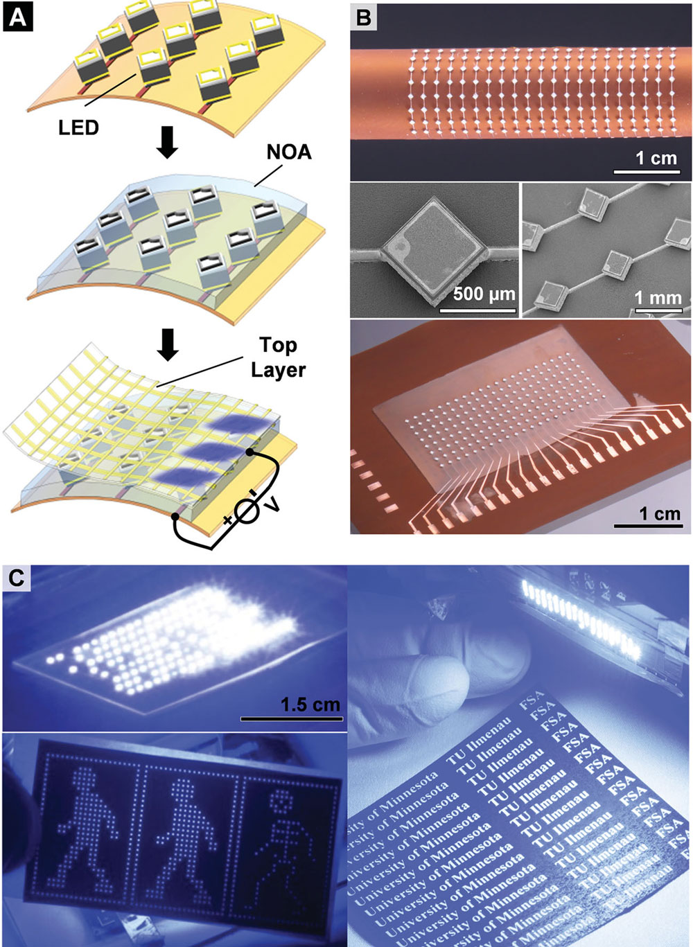
| As a demonstration, the researchers applied their self-assembly machine to the realization of area lighting panels incorporating distributed inorganic light emitting diodes (GaN LEDs). The lighting modules are fabricated in three steps: 1) assembly of LEDs on the bottom electrode using the RTR system; 2) isolation and passivation of assembled LEDs with UV curable polymer; and 3) lamination of top conductive layer to complete the electrical connections (see figure below). | |
 |
|
| RTR fluidic self-assembly system applied to the fabrication of area lighting modules. (A) Fabrication procedure: assembly of LED using the RTR fluidic self-assembly system, area isolation and passivation of assembled LEDs with UV curable polymer (NOA), and lamination of top conductive layer. (B) Optical photograph of assembled LEDs wrapped onto a cylinder (top), SEM close-ups (middle), and optical photograph after isolation using UV curable polymer (bottom). (C) Application as lighting panel (left, top), backlighting unit (left, bottom), and area illumination unit (right). (Reprinted with permission by Wiley-VCH Verlag) (click on image to enlarge) | |
| Although this is still basic research, Jacobs and his collaborators have set their eyes on the development of industrial-scale 'self-assembly machines' which would allow the assembly and electrical interconnection of semiconductor chips over wide area substrates in large quantities with high speed and high precision. | |
| "I am convinced that processes of self-assembly will eventually be used in the manufacturing industry of the future," says Jacobs. "Today it might appear as science-fiction to some critical observers. However, researchers worldwide including my group continue to work out the details." | |
 By
Michael
Berger
– Michael is author of three books by the Royal Society of Chemistry:
Nano-Society: Pushing the Boundaries of Technology,
Nanotechnology: The Future is Tiny, and
Nanoengineering: The Skills and Tools Making Technology Invisible
Copyright ©
Nanowerk LLC
By
Michael
Berger
– Michael is author of three books by the Royal Society of Chemistry:
Nano-Society: Pushing the Boundaries of Technology,
Nanotechnology: The Future is Tiny, and
Nanoengineering: The Skills and Tools Making Technology Invisible
Copyright ©
Nanowerk LLC
|
|
|
Become a Spotlight guest author! Join our large and growing group of guest contributors. Have you just published a scientific paper or have other exciting developments to share with the nanotechnology community? Here is how to publish on nanowerk.com. |
|