| Posted: Nov 05, 2014 | |
Fully 3D-printed quantum dot LEDs |
|
| (Nanowerk Spotlight) To date, the 3D printing of electronic components has been limited to the printing of batteries, strain sensors, interdigitated-electrode capacitors and passive metallic structures such as interconnects and antennas on surfaces or within biological organs. | |
| The ability to directly and seamlessly incorporate materials with a range of diverse functionalities with 3D printing is particularly attractive as it could allow the simultaneous, comprehensive, and direct printing of structural, biological, and electronic materials that capture the complete spectra of material properties. | |
| The free-form generation of active electronics in unique architectures which transcend the planarity inherent to conventional microfabrication techniques has been an area of increasing scientific interest. Yet, attaining seamless interweaving of electronics is challenging due to the inherent material incompatibilities and geometrical constraints of traditional micro-fabrication processing techniques. | |
| At the fundamental level, 3D printing should be entirely capable of creating spatially heterogeneous multi-material structures by dispensing a wide range of material classes with disparate viscosities and functionalities, including semiconducting colloidal nanomaterials, elastomeric matrices, organic polymers, and liquid and solid metals. | |
| "The big push in 3D printing these days is to try to print two or more polymers at once," Michael McAlpine, an assistant professor of mechanical and aerospace engineering at Princeton University, tells Nanowerk. "In our latest research, we go way beyond that. We show that we can print interwoven structures of quantum dots, polymers, metal nanoparticles, etc, to create the first fully 3D printed LEDs, in which every component is 3D printed." | |
| This demonstration represents a proof of concept in combining active nanoelectronic components with the versatility of 3D printing, which enables the three-dimensional free-form fabrication of active electronics. | |
 |
|
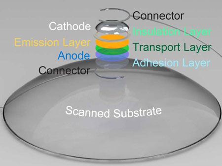
| 3D printed quantum dot light-emitting diode (QLED) on a 3D scanned curvilinear substrate. This CAD model shows the QD-LED components and conformal integration onto the curvilinear substrate. (Reprinted with permission by American Chemical Society) | |
| McAlpine and his team published their findings in Nano Letters ("3D Printed Quantum Dot Light-Emitting Diodes"). | |
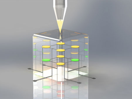
| "Using this approach, we can create unique structures, such as 2x2x2 arrays of LEDs, in which the electrical wiring runs horizontal and vertical, to create a multi-color 3D stack of LEDs," notes Yong Lin Kong, a graduate student in McAlpine's group who led this project and first author of the paper. "We also use 3D scanning to carefully scan a contact lens and store the specific topology of that lens, and then alter our 3D printing to adjust to that topology, allowing us to conformally 3D print LEDs on a contact lens. This may have use in electronic contact lens or bionic eye applications in the future." | |
| "This work outlines an exciting breakthrough that enables the direct printing of functional, embedded, active 3D nanoelectronics using only a 3D printer," he adds. "Indeed, this is the first time to our knowledge that semiconducting nanoparticles have been 3D printed, and the first time that such a broad array of diverse functional materials have been fully interwoven entirely using a 3D printer." | |
| The team's approach consists of three key steps. First, it identifies electrodes, semiconductors, and polymers that possess desired functionalities and exist in printable formats. Next, care is taken to ensure that these materials are dissolved in orthogonal solvents so as not to compromise the integrity of underlying layers during the layer-by-layer printing process. Finally, the interwoven patterning of these materials is achieved via direct dispensing in a CAD-designed construct. | |
| As a proof of concept of this approach, the researchers demonstrate the 3D printing of quantum dot light-emitting diodes (QLEDs), which involves the design, integration and printing of five classes of materials with distinct material properties. | |
| "Specifically, we demonstrate the seamless interweaving of 1) emissive semiconducting inorganic nanoparticles; 2) an elastomeric matrix; 3) organic polymers as charge transport layers; 4) solid and liquid metal leads; and 5) a UV-adhesive transparent substrate layer," explains Kong. "The printed QLEDs exhibit excellent performance characteristics. The combination of 3D scanning and 3D printing allows for the direct printing of active functional electronics onto the precise topology of a non-flat object." | |
 |
|
| 3D printed multidimensional array of embedded QD-LEDs. (A) Layout of the multi-color 3D QD-LED array design. (Image: McAlpine Group) | |
| He points out that, most excitingly, this approach allows for the free-form fabrication of multi-dimensional nanoelectronics within a complex, interwoven architecture such as a 3D array of embedded QLEDs. | |
| The QLEDs printed by McAlpine's team capture the unique properties of quantum dots: tunable and pure color emission. Further, combining a complementary 3D light-scanning technique with this approach allows for the fabrication of electronics topographically tailored to curvilinear surfaces. | |
| "We anticipate that this general strategy can be expanded to 3D print other classes of active devices, such as MEMS devices, transistors, solar cells, and photodiodes," says McAlpine. "Our results suggest a number of exciting applications, including the generation of geometrically tailored devices containing LEDs and multimodal sensors to provide a new tool for optogenetics for studying neural circuitry." | |
| Co-printing of active electronics with biological constructs could also lead to new bionic devices, such as prosthetic implants that optically stimulate nerve cells. | |
| According to the team, future work will address a number of key challenges. These include: 1) increasing the resolution of the 3D printer such that smaller devices can be printed; 2) improving the performance and yield of the printed devices; and 3) incorporating other classes of nanoscale functional building blocks and devices, including semiconductor, plasmonic, and ferroelectric. | |
 By
Michael
Berger
– Michael is author of three books by the Royal Society of Chemistry:
Nano-Society: Pushing the Boundaries of Technology,
Nanotechnology: The Future is Tiny, and
Nanoengineering: The Skills and Tools Making Technology Invisible
Copyright ©
Nanowerk LLC
By
Michael
Berger
– Michael is author of three books by the Royal Society of Chemistry:
Nano-Society: Pushing the Boundaries of Technology,
Nanotechnology: The Future is Tiny, and
Nanoengineering: The Skills and Tools Making Technology Invisible
Copyright ©
Nanowerk LLC
|
|
|
Become a Spotlight guest author! Join our large and growing group of guest contributors. Have you just published a scientific paper or have other exciting developments to share with the nanotechnology community? Here is how to publish on nanowerk.com. |
|