| Posted: Nov 27, 2014 | |
3D printed nanostructures made entirely of graphene |
|
| (Nanowerk Spotlight) Graphene has received a great deal of attention for its promising potential applications in electronics, biomedical and energy storage devices, sensors and other cutting-edge technological fields, mainly because of its fascinating properties such as an extremely high electron mobility, a good thermal conductivity and a high elasticity. | |
| The successful implementation of graphene-based devices invariably requires the precise patterning of graphene sheets at both the micrometer and nanometer scale. Finding the ideal technique to achieve the desired graphene patterning remains a major challenge. | |
| 3D printing, also known as additive manufacturing, is becoming a viable alternative to conventional manufacturing processes in an increasing number of applications ranging from children toys to cars, fashion, architecture, military, biomedical science, and aerospace, to name a few. | |
| For the first time, researchers have now demonstrated 3D printed nanostructures composed entirely of graphene using a new 3D printing technique. The research team, led by Professor Seung Kwon Seol from Korea Electrotechnology Research Institute (KERI), has published their findings in the November 13, 2014 online edition of Advanced Materials ("3D Printing of Reduced Graphene Oxide Nanowires") | |
| "We developed a nanoscale 3D printing approach that exploits a size-controllable liquid meniscus to fabricate 3D reduced graphene oxide (rGO) nanowires," Seol explains to Nanowerk. "Different from typical 3D printing approaches which use filaments or powders as printing materials, our method uses the stretched liquid meniscus of ink. This enables us to realize finer printed structures than a nozzle aperture, resulting in the manufacturing of nanostructures." | |
 |
|
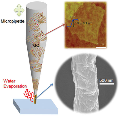
| Schematic diagram of GO nanowire fabrication by pulling a micropipette filled with an aqueous GO suspension (GO sheet thickness = 0.9 ± 0.1 nm) and stretching the meniscus during water evaporation. In the circle (lower right): FE-SEM image showing a grown rGO nanowire with r = 400 nm. (Reprinted with permission by Wiley-VCH Verlag) | |
| The researchers note that their novel solution-based approach is quite effective in 3D printing of graphene nanostructures as well as in multiple-materials 3D nanoprinting. | |
| "We are convinced that this approach will present a new paradigm for implementing 3D patterns in printed electronics," says Seol. | |
| For their technique, the team grew graphene oxide (GO) wires at room temperature using the meniscus formed at the tip of a micropipette filled with a colloidal dispersion of GO sheets, then reduced it by thermal or chemical treatment (with hydrazine). | |
| The deposition of GO was obtained by pulling the micropipette as the solvent rapidly evaporated, thus enabling the growth of GO wires. The researchers were able to accurately control the radius of the rGO wires by tuning the pulling rate of the pipette; they managed to reach a minimum value of ca. 150 nm. | |
| Using this technique, they were able to produce arrays of different freestanding rGO architectures, grown directly at chosen sites and in different directions: straight wires, bridges, suspended junctions, and woven structures. | |
| This video shows the formation of a freestanding GO nanowire. | |
| "So far, to the best of our knowledge, nobody has reported 3D printed nanostructures composed entirely of graphene," says Seol. "Several results reported the 3D printing (millimeter- or centimeter-scale) of graphene or carbon nanotube/plastic composite materials by using a conventional 3D printer. In such composite system, the graphene (or CNT) plays an important role for improving the properties of plastic materials currently used in 3D printers. However, the plastic materials used for producing the composite structures deteriorate the intrinsic properties of graphene (or CNT)." | |
| He points out that this 3D nanoprinting approach can be used for manufacturing 2D patterns and 3D architectures in diverse devices such as printed circuit boards, transistors, light emitting devices, solar cells, sensors and so on. Reducing the 3D printable size to below 10 nm and increasing the production yield still remain challenges, though. | |
 By
Michael
Berger
– Michael is author of three books by the Royal Society of Chemistry:
Nano-Society: Pushing the Boundaries of Technology,
Nanotechnology: The Future is Tiny, and
Nanoengineering: The Skills and Tools Making Technology Invisible
Copyright ©
Nanowerk LLC
By
Michael
Berger
– Michael is author of three books by the Royal Society of Chemistry:
Nano-Society: Pushing the Boundaries of Technology,
Nanotechnology: The Future is Tiny, and
Nanoengineering: The Skills and Tools Making Technology Invisible
Copyright ©
Nanowerk LLC
|
|
|
Become a Spotlight guest author! Join our large and growing group of guest contributors. Have you just published a scientific paper or have other exciting developments to share with the nanotechnology community? Here is how to publish on nanowerk.com. |
|