| Posted: Feb 01, 2008 | |
Organic molecular nanotechnology |
|
| (Nanowerk Spotlight) The vision of revolutionary bottom-up nanotechnology is based on a concept of molecular assembly technologies where nanoscale materials and structures self-assemble to microscale structures and finally to macroscopic devices and products. | |
| We are a long way from realizing this vision but researchers are busily laying the foundation for nanoscale engineering. Assembling nanoscopic components into macroscopic materials is an appealing goal but one of the enormous difficulties lies in bridging approximately six orders of magnitude that separate the nanoscale from the macroscopic world. | |
| Until machinery capable of automated and industrial-scale nano-assembly can be built, the parallelism of chemical synthesis and self-assembly is necessary when controlling materials at the nanoscale. An obvious direct approach to molecular nanotechnology therefore is to start with organic molecules as building blocks. | |
| Modest from the viewpoint of molecular manufacturing visionaries, but quite fascinating to a lot of scientists, research into nanofibers, as a modification of organic crystals, is making good progress. New research results coming out of Denmark offer the basis for a novel organic-molecule-based nanotechnological concept that allows for a multitude of applications in fundamental research and in device applications. | |
| Essentially, this concept is based on three steps: 1) directed self-assembled surface growth of nanofibers from functionalized molecules; 2) transfer and manipulation of individual fibers as well as of ordered arrays; and 3) device integration. | |
| "Work in our group has allowed us to overcome the previous obstacles of growing molecular nanowires – namely the controlled growth of crystallites of predefined shapes and predefined mutual orientations and their transfer onto more complicated target substrates" Dr. Horst-Günther Rubahn tells Nanowerk."The result is an organic molecular nanotechnology that allows for the generation of mutually aligned, morphologically well-defined light-emitting organic nanofibers from functionalized molecules, essentially bridging the gap between the nanoscopic and microscopic worlds. Our nanofibers can be transferred easily and destruction-free as individual entities or in a massive parallel fashion onto pre-structured target substrates. Due to their crystalline perfection and due to the morphological control, organic nanofibers are perfectly suited for fundamental studies of optics, mechanics, and electronics on the mesoscale. Applications as passive and active elements in printed all-optical chips are within reach." | |
| The work of Rubahn, a professor at the University of Southern Denmark's Mads Clausen Institute, and his collaborators from the University of Oldenburg and the University of Bonn, both in Germany, advances bottom-up nanotechnology since it shows that it is possible to generate on a large scale well-oriented and well-defined nanostructures, the properties of which can be modified at will. | |
| "In addition" says Rubahn, "discontinuous growth of the kind demonstrated in our work is interesting per se for a better control of organic thin film growth. Such control, in turn, is most relevant for future organic electronics and photonics – from flat screens to photonic circuits." | |
| In their paper in the January 18, 2008 online edition of Small ("Organic Molecular Nanotechnology") the scientists introduce their three-step concept that provides a new route to bottom-up organic nanotechnology. | |
| Step 1: In their work the researchers came to the conclusion that the growth of oriented nanofibers from functionalized quaterphenylenes on muscovite mica is a generic process that can be performed with a variety of different functionalizations of quaterphenylenes. | |
| "The ordered form of discontinuous organic molecular film growth forms the basis of our nanotechnological concept" says Rubahn. "Our detailed investigations have shown that the growth of large, parallel oriented fibers or 'needles' is due to the unique combination of an atomically flat, single-crystalline growth substrate with large electric dipole domains and molecules that fulfill, in their crystalline bulk form, quasiepitaxial relationships between adsorbate and substrate." | |
| He describes the second step of their nanotechnological concept as the detachment, controlled transfer, and mechanical manipulation of the as-grown nanofibers. "By using an appropriate combination of liquid, external energy, and specific surface morphology, nanofibers can be stamped as single entities or as ordered arrays onto storage media and from there onto arbitrary substrates" Rubahn explains. "Alternatively, they can be transferred into liquids or gels for further manipulation. These manipulation processes appear to be working for functionalized nanofibers as well and they take great advantage of the chemical inertness and thermal stability of the nanofibers." | |
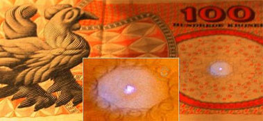
| Finally, in step three – due to the ease of nanofiber transfer – numerous possibilities for device integration come into technological reach. Rubahn cites examples such as the transfer of individual fibers onto optoelectronic circuits for electroluminescence applications or mass transfer of nanofiber arrays onto precious documents, such as banknotes, for security purposes. | |
| "It is important to note that neither the individual nor the mass transfer process mechanically affects the morphology of the nanofibers, thus their specific properties (dichroism, waveguiding, optical resonance) are fully functional on the new substrate" says Rubahn. | |
| The research team also points out that their novel concept is related to the morphology of the organic nanofibers as well as their high degree of crystallinity and the specific orientation of the molecular building blocks. The result is a new class of materials of on a nanoscale morphologically tailored fibers with specific optoelectronic and chemical properties. | |
| Typical widths of the nanofibers range from less than a hundred to a few hundred nanometers with heights of the order of a few tens of nanometers and lengths between a few hundred nanometers and a millimeter. Since the nanofibers are emitting intense visible light they are obvious candidates for basic nanophotonic investigations. | |
  |
|
| Stamped nanofibers onto a banknote form a blue-light-emitting triangle, which appears due to waveguiding and crystalline stacking more brilliant when seen from the side (right) as compared to the appearance from above. (Images: Dr. Rubahn, University of Southern Denmark) | |
| The list of potential applications includes nanoscale frequency doublers, nanolasers with low threshold, generic nanosensor platforms etc. Rubahn has set up a company – >Nanofiber A/S — to commercialize his research on organic nanofibers. One of the company's first products are security markers that incorporate organic nanofibers, called 'nanomarkers.' | |
| The work of Rubahn's team has opened the way for new materials for advanced applications such as core/shell wires and segmented nanowires from different organic materials or even from combinations of organic and inorganic compounds. For now, there are still some basic challenges to be overcome, such as the stability of the organic material as well as investigating the potential toxicity of the nanofibers. | |
| Nevertheless, Rubahn is confident that a more thorough understanding of growth and stability of their nanofibers will eventually lead to the tailored growth of nanoaggregates via surface structure formation. | |
 By
Michael
Berger
– Michael is author of three books by the Royal Society of Chemistry:
Nano-Society: Pushing the Boundaries of Technology,
Nanotechnology: The Future is Tiny, and
Nanoengineering: The Skills and Tools Making Technology Invisible
Copyright ©
Nanowerk LLC
By
Michael
Berger
– Michael is author of three books by the Royal Society of Chemistry:
Nano-Society: Pushing the Boundaries of Technology,
Nanotechnology: The Future is Tiny, and
Nanoengineering: The Skills and Tools Making Technology Invisible
Copyright ©
Nanowerk LLC
|
Become a Spotlight guest author! Join our large and growing group of guest contributors. Have you just published a scientific paper or have other exciting developments to share with the nanotechnology community? Here is how to publish on nanowerk.com.