| Posted: Feb 06, 2017 | |
Lego like silicon electronics fabricated with hybrid etching masks |
|
| (Nanowerk Spotlight) Bulk micromachining techniques are commonly used for making high aspect ratio structures used in complementary metal oxide semiconductor (CMOS) technology, microelectromechanical systems (MEMS), dynamic random access memory (DRAM) capacitors, and 3D integrated circuits. These techniques generally utilize a hard mask – for example metal – material to withstand abrasive deep reactive ion etching (DRIE) that is used in bulk micromachining. | |
| However, the use of hard masks during deep etching (hundreds of microns) imposes some manufacturing limitations. A novel technique eliminates the disadvantages of using hard mask alone, which (a) can diffuse into the lower layers; (b) is hard to etch or etched using chemicals that are not environment friendly or convenient for device fabrication due to contamination and selectivity; and (c) affects the surface roughness of underlying layers during deposition and etching. | |
| "The novelty of our technique is the combination of using a soft and hard mask together in a single entity (a hybrid mask) during the deep etching and the reaped benefits in terms of combining resistance to prolonged etching, easy removal, and preservation of lower layers simultaneously," Muhammad Mustafa Hussain, an Associate Professor of Electrical Engineering at King Abdullah University of Science and Technology (KAUST), explains to Nanowerk. | |
| The different properties of positive and negative photoresist (photosensitive materials) in terms of how they respond to light and interact with developer chemicals can be used to transform one of them into an actual masking layer (sacrificial). For instance, if a negative photoresist is exposed to ultra-violet (UV) light it becomes insoluble in developer. | |
| This enabled the KAUST team to deposit and pattern another mask (hard mask) using positive photoresist and patterning the positive photoresist in developer without affecting the negative photoresist – which is insoluble in developer after UV exposure and separated by a hard mask from the positive photoresist. | |
| The researchers have published their findings in Small ("Highly Manufacturable Deep (Sub-Millimeter) Etching Enabled High Aspect Ratio Complex Geometry Lego-Like Silicon Electronics"). | |
 |
|
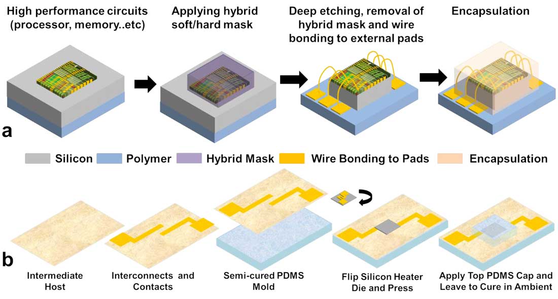
| (a) Conceptual design of flexible packaging of high performance electronics using hybrid soft/hard mask etching technique, (b) utilized flow for packaging sample die in PDMS. (Reprinted with permission by Wiley-VCH Verlag) (click on image to enlarge) | |
| "Our hybrid mask combines the advantages of each layer," notes Mohamed Tarek Ghoneim, first author of the paper. "Having a sacrificial layer and a hard mask on top brings has two major benefits: 1) The hard mask exposed to the etching plasma/gases is strong enough to persist deep long etches; and 2) the sacrificial layer is easily etched away and consequently wipes the hard mask alongside." | |
| Having a sacrificial layer that is made of soft materials, such as polymers or traditional photoresists, preserves the surface roughness of underlying layers, does not contaminate or diffuse ions into lower layers, and is easily removed by immersion in organic solvents, such as acetone. | |
| As the team points out, using the hybrid mask enables deep sub-millimeter etching while preserving existing devices and structures and is advantageous for many applications, including precise dicing, making irregular shaped dies, and novel packaging techniques – including lego like concept for pre-packaging modules/system integration. | |
| This novel technique should be seen as an addition to the available dicing techniques and deep etching in general. It eliminates previous restrictions on material systems imposed due to the challenges of using a soft or hard mask separately, enabling a wider material system choices for further optimization of valuable device/system parameters. | |
| Furthermore, it will open new possibilities for novel packaging techniques and reduce the environmental impact of micro fabrication etching/patterning processes, including non-deep etches. | |
| As with many innovations, this one also was based on quite a bit of trial and error. Hussain recounts his experience: "The motivation was my previous failed attempts to conduct the deep etching for another project aimed at using micro-fabrication techniques to build deep micro structures in silicon for heat dissipation in order to replace the need for bulky heat sinks in wearable and flexible electronics. | |
| "First, I used polymer masks which were gone long before the etch was complete. Then, I used hard masks which solved the long etch issue but presented the difficulty in removing hard mask afterwards in terms of the strong chemicals needed, contamination issues and surface roughness of underlying layers. | |
| "Then, I thought about the advantages/disadvantages of each approach and found that they are actually complementary to each other not alternatives. After brainstorming, I got the idea of using the different properties of negative and positive photosensitive materials to turn one into a mask layer and use the other to pattern a hard mask layer. Demonstration of the concept and representative applications followed. " | |
 |
|
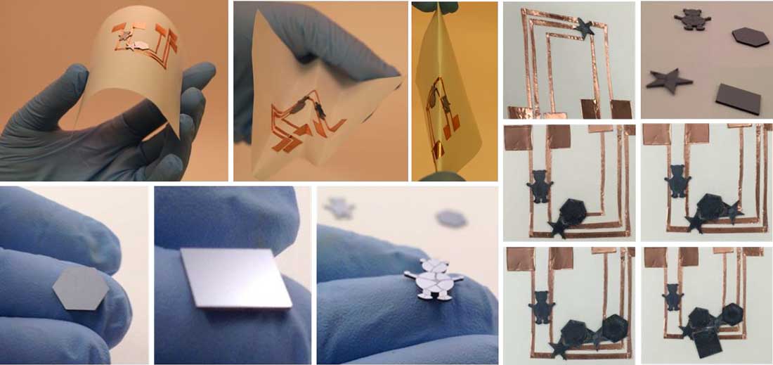
| Diced asymmetric patterns using hybrid soft/hard mask for deep etching. The cracks around sharp angles are subject of further optimizations and they should not affect the devices on the other side. Top left images show the Lego dies on flexible substrate with interconnects. Side images show connection strategy and Lego concept for fitting dies on underlying interconnects. (Reprinted with permission by Wiley-VCH Verlag) (click on image to enlarge) | |
| Going forward, Hussain and his group will investigate further optimization for irregular dicing, and attempt to demonstrate a pre-packaging Lego-like electronics concept to connect various electronic systems modules at the die level using their deep etching technique to turn traditional silicon dies into lego pieces. | |
| Furthermore, they will seek to adapt their technique for even non-deep etches to reap its process simplification/lower layer preservation benefits and assessing the limitations in terms of minimum lateral feature achievable as a function of depth for (shallow etches). | |
 By
Michael
Berger
– Michael is author of three books by the Royal Society of Chemistry:
Nano-Society: Pushing the Boundaries of Technology,
Nanotechnology: The Future is Tiny, and
Nanoengineering: The Skills and Tools Making Technology Invisible
Copyright ©
Nanowerk LLC
By
Michael
Berger
– Michael is author of three books by the Royal Society of Chemistry:
Nano-Society: Pushing the Boundaries of Technology,
Nanotechnology: The Future is Tiny, and
Nanoengineering: The Skills and Tools Making Technology Invisible
Copyright ©
Nanowerk LLC
|
|
|
Become a Spotlight guest author! Join our large and growing group of guest contributors. Have you just published a scientific paper or have other exciting developments to share with the nanotechnology community? Here is how to publish on nanowerk.com. |
|