| Posted: May 11, 2017 | |
Bubble-printed patterning of quantum dots on plasmonic substrates |
|
| (Nanowerk Spotlight) The use of quantum dots (QDs) in practical applications relies on the ability to precisely pattern QDs on substrates with desired optical properties. Typical direct-write printing techniques such as inkjet and gravure printing are limited in resolution (micron-scale), structural complexity, and require significant post-processing time. | |
| In new work, researchers at the University of Texas at Austin use laser-induced bubble printing to pattern CdSe/CdS QDs on plasmonic substrates with submicron resolution (<700nm line width), high throughput (∼104 µm/s) and strong QD-substrate adhesion. | |
| Not only is the bubble-mediated immobilization at the submicron scale stable, but the submicron-sized bubble's stability can be maintained over a large area. | |
| This technique is also compatible with flexible substrates and can be further integrated with smartphone to realize haptic integration. Finally, the emission characteristics of the QDs in terms of the emission wavelength and lifetime can be modified in real-time to achieve site-sensitive emission. | |
| The team, led by Yuebing Zheng, Assistant Professor of Mechanical Engineering and Materials Science & Engineering has been published in ACS Applied Materials & Interfaces ("High-Resolution Bubble Printing of Quantum Dots"). | |
 |
|
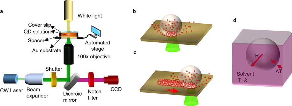
| Working principle of bubble printing (BP) of QDs on plasmonic substrates. (a) Schematic of the optical setup for BP. (b) Schematic showing the QDs being trapped toward the bubble generated on the substrate and the eventual immobilization of QDs on the substrate. (c) Illustration of the QDs immobilized along the path traversed by the laser beam to create patterns of QDs on the substrate. (d) Schematic illustration of the different parameters that affect the outward heat flux and the bubble generation. T, solvent temperature; k, solvent thermal conductivity; R, radius of the bubble; ΔT, temperature difference across bubble surface. (Reprinted with permission by American Chemical Society) (click on image to enlarge) | |
| "The direct-print techniques can provide real-time configurability as well as reduce significant overhead costs for mask fabrication," Bharath Bangalore Rajeeva, the paper's first author, tells Nanowerk. "The submicron printing capability achieved in this work is critical to fabricate ultra-high resolution displays, biosensors with small footprints, anti-counterfeiting micro-QR codes, and nanolasers. In addition, the emission tuning capability can be used as an encoding scheme to produce distinguishable optical codes." | |
| In order to achieve the QD patterning on plasmonic substrates, the team utilized microbubble-mediated immobilization, thereby circumventing the challenges of other direct-print techniques such as achievement of submicron resolution, ink spreading and long drying times post deposition. | |
| Watch a video of the bubble-printing technique. (Video: Zheng Research Group, UT Austin) | |
| The printing parameters can be optimized to further control the fluorescence properties of the patterned QDs such as emission wavelength and lifetime. | |
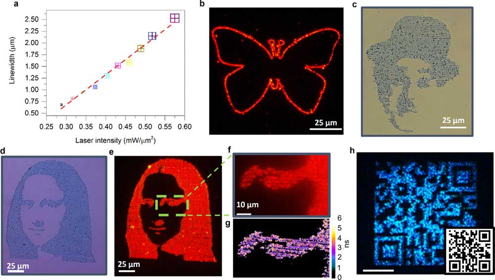
| As proof of concept of their new technique, the researchers demonstrated high-resolution intricate patterns of QDs resembling famous personalities such as Charlie Chaplin, Mona Lisa and microscale QR code with dimension of 120 µm x 90 µm, 150 µm x 90 µm, and 80 µm x 80 µm, respectively. | |
| The researchers point out that bubble printing can achieve similar printing parameters on flexible substrates. | |
| "For the next steps, we aim to extend the bubble printing technique to other nanoparticle systems to create functional devices such as nano/micro scale sensors and waveguides," notes Zheng. "Further reduction in bubble size and increase of throughput is a parallel direction to be explored." | |
 |
|
| Versatile BP capabilities: (a) Plot of pattern line width vs incident laser intensity. The linear fitting shows the on-demand capability of tuning the patterning dimensions by the laser power. (b) BP of red QDs into a contour of a butterfly, as shown in fluorescence image. The line width is 1 µm. (c) Bright-field image of a Charlie Chaplin pattern of QDs via raster scanning in BP. The overall size is 120 µm x 90 µm with 1 µm line space. (d, e) Bright-field and fluorescence images tetramethylrhodamine isothiocyanate filter set) of Mona Lisa printed with red QDs using a raster scanning approach. The size of the complete image is 150 µm x 90 µm. (f) Magnified fluorescence image depicting the high-resolution patterning capability of BP. (g) FLIM of the QDs showing high-density uniform patterning capability of BP. (h) Fabrication of a microscale (80 µm x 80 µm) QR code with blue QDs printed via raster scanning. The scale bar is 25 µm. (Reprinted with permission by American Chemical Society) (click on image to enlarge). Note: The QR code in the image actually works – check it out. | |
| The technique is also compatible with smartphone integration, and the corresponding work has been recently reported as haptic-interfaced bubble printing in Journal of Materials Chemistry C ("Patterning and fluorescence tuning of quantum dots with haptic-interfaced bubble printing"). | |
| Future work by the team will investigate other nanoparticle systems to realize functional devices, such as colloidal nanosensors, flexible LED microdisplay devices, as well as colloidal waveguides, and to test the limits of this technique in-terms of bubble stability and printing throughput. | |
| Further applications such as flexible electronics, flexible photonics, and biological applications could also be pursued. The critical challenges to be addressed include the improvement of the line-roughness and extension towards three-dimensional printing. | |
 By
Michael
Berger
– Michael is author of three books by the Royal Society of Chemistry:
Nano-Society: Pushing the Boundaries of Technology,
Nanotechnology: The Future is Tiny, and
Nanoengineering: The Skills and Tools Making Technology Invisible
Copyright ©
Nanowerk LLC
By
Michael
Berger
– Michael is author of three books by the Royal Society of Chemistry:
Nano-Society: Pushing the Boundaries of Technology,
Nanotechnology: The Future is Tiny, and
Nanoengineering: The Skills and Tools Making Technology Invisible
Copyright ©
Nanowerk LLC
|
|
|
Become a Spotlight guest author! Join our large and growing group of guest contributors. Have you just published a scientific paper or have other exciting developments to share with the nanotechnology community? Here is how to publish on nanowerk.com. |
|