| Posted: Jun 09, 2017 | |
A two-dimensional electron microscope inside graphene |
|
| (Nanowerk Spotlight) The electron microscope has been humanity’s most important magnifying glass, since the first electron lens was invented in 1926 by Hans Busch. Just five years later, the first electron microscope was constructed, nearly 90 years ago. The much smaller wavelength of high energy electrons compared to light, meant that a whole new world was now “open for inspection” – the micro- and nanoscale. | |
| Modern-day electronics or communication technology would not exist without electron microscopy, and the same can be said for many other types of technology. Since then, electron microscopes have evolved into a multitude of powerful techniques, that allow even individual atoms to be imaged. | |
| Beyond imaging, the focused beam of electrons is also used for analysis of the chemical composition of materials, their crystal structure, and many other useful things. | |
| With the discovery of graphene, an atomically thin sheet of carbon atoms with unique and powerful properties, electron microscopy has a chance to enter “flatland”. Electrons moving in solids take on different behaviors depending on the properties of the solid – they become quasiparticles. | |
| The quasiparticle in graphene is called a Dirac fermion, and resembles more a photon than an electron. For instance, Dirac fermions move at a constant speed regardless of the energy, 300 times slower than the speed of light. | |
| One consequence of these “light-like” properties is the suppression of scattering. In graphene, electrons can move more than a micrometer between collisions at room temperature, and when cooled down, up to 30 µm and maybe even longer. Graphene is like 'vacuum' for electrons. | |
 |
|
| (adapted from Bøggild et al, Nature Communications) (click on image to enlarge) | |
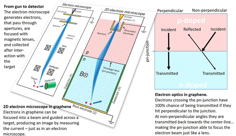
| Researchers at the Technical University of Denmark and RWTH Aachen University in Germany have proposed to use graphene as a two-dimensional vacuum chamber, and build a two-dimensional electron microscope, where the electrons fly from the electron gun to the target without ever leaving the graphene sheet. | |
| Such an instrument could be used to study the scattering behavior of electrons in graphene devices, the edges of graphene, and the interaction between graphene and objects (particles, quantum dots, antennas) deposited on the surface – which is commonly used to augment and tune the behavior of graphene devices. | |
| This is not as crazy as it sounds. Electron optics in graphene was suggested for the first time 10 years ago, when it was pointed out that electrons that move from an electron rich region (n-doped) to an electron-deprived region (p-doped), where the carriers are called 'holes' (missing electrons), a process that is called 'Klein Tunneling'. | |
| The peculiar rules of graphene optics with pn-junctions can be summarized: | |
|
|
|
| This makes a single pn-junction act as a focusing lens or as other powerful optical components. In the past few years, leading research groups in Korea, Europe and US have demonstrated electron optics do work, in a series of elegant and beautiful experiments. | |
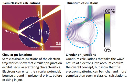
| The DTU group, led by Peter Bøggild, carried out calculations both with semiclassical (raytracing) and quantum mechanical simulations, to prove the basic concept, and explore how far the analogy between two-dimensional and three-dimensional electron microscopes can be pushed. Using a point contact and an aperture to mimic the electron source, pn-junctions to build focusing and collimating lenses, and large electrodes to pick up electrons after hitting the target – all that is left is a weak magnetic field to gently deflect the electron beam and allow it to scan across the target. | |
| The simulations show that the high-performance graphene devices and the existing electron optics components is sufficient to make it work in practice, and that the focused electron beam could indeed be used to probe not just the shape, but also the electronic properties of edges as well as deposited objects on top of the graphene. | |
 |
|
| (adapted from Bøggild et al, Nature Communications) | |
| One object of particular interest for the team was a circular pn-junction. Since electrons can penetrate the barrier by Klein tunneling, electronic states can be excited inside the cavity (think of standing sound waves in a closed room) – leading to strange current emission patterns, as the rules of electrons escaping from the circular potential are governed by the strong angular dependence of the Klein tunneling. | |
| Peter Boggild got the idea for the microscope while preparing a lecture on electron microscopy, while also writing a research proposal on ballistic transport in graphene: "Many of the components in electron microscopy, happen to have a counterpart in graphene electronics, so we started to explore the 2D electron microscope on a conceptual level. Now we will try to build one." | |
| Boggild does not know yet how well this will work: "We shall see whether this particular apparatus can tell us anything important, but there are so many wonderful things you could do with focused beams of electrons in graphene. We are having a great time coming up with devices that rely on focused spin-polarized electron beams, coherent electron beams or perhaps time-resolved measurements. Short bursts of focused electron beams could be detected picoseconds later with femtosecond time-resolution, after having passed through a graphene device. Since the carriers all move at the same velocity, the temporal response could tell us what the electrons did while passing through device – think for instance of echoes." | |
| Christoph Stampfer from RWTH Aachen elaborates: "It is very exciting to think that fundamental studies of ballistic electron transport are potentially leading to a new experimental tool – the 2D electron microscope – offering new possibilities to investigate nature." | |
| Other areas considered by the team is the use of electron optics to improve make room-temperature ballistic electronics, to provide faster switching and more complex functionality compared to present-day semiconductor based components. | |
| This video shows a simulation of the microscope as it scans a circular pn-junction. | |
| The work is published in Nature Communications ("A two-dimensional Dirac fermion microscope") and sponsored by the DNRF Center of Nanostructured Graphene and the European Graphene Flagship project. | |
|
Source: Provided as a Nanowerk exclusive by Technical University of Denmark (DTU)
|
|
|
Become a Spotlight guest author! Join our large and growing group of guest contributors. Have you just published a scientific paper or have other exciting developments to share with the nanotechnology community? Here is how to publish on nanowerk.com. |
|