| Posted: Sep 30, 2008 | |
Nanotechnology skin to rival human touch |
|
| (Nanowerk Spotlight) Artificial skin already exists that can detect pressure and recently, thanks to carbon nanotube rubber, it now even is stretchable (see: Carbon nanotube rubber could provide e-skin for robots). Then there is stretchable artificial skin that is used, for instance, to provide grafts for human burns victims, but it is insensitive to heat and pressure. Skin-like sensitivity, or the capability to recognize tactile information, will be an essential feature of future generations of robots. Of course you could also dream up some sci-fi scenarios where artificial electronic skin vastly enhances human perception and performance. The development of electronic skin requires high-performance tactile sensors that mimic human skin in terms of touch sensation over a large area, high flexibility, resolution, and sensitivity comparable to a human finger, as well as ease of signal extraction for speed and implementation. A recent review article summarizes the current state of developing artificial touch, an area where significant progress has been made over the past few years. | |
| Vivek Maheshwari and Ravi Saraf write in their review ("Tactile Devices To Sense Touch on a Par with a Human Finger") that sensor devices are critical to the development of tools that can enhance or replace human intervention, for instance in minimally invasive surgery or robotics. They describe how recent developments in materials chemistry, nanotechnology, and single-molecule devices have great potential in improving the current technology significantly. | |
| "Sensors interface with the environment, similar to the five human senses of hearing, smell, touch, vision, and taste, to stimulate a suitable response or action. Among the first four senses, touch remains the most challenging sense to emulate, where capabilities on a par with a human finger are required. The difficulty lies in designing a high-resolution device that can be mounted on a curved surface and also sense a distribution of stimuli at high spatial resolution over a large area of contact. For example, a human finger – the most sensitive touch sensor known – can feel texture by detecting surface roughness at a spatial resolution of about 40 µm over a contact-area of approximately 1 square centimeter and at stress levels of 10–40 KPa; in contrast, current sensor devices have a resolution of 2 mm for a similar contact area." | |
| One of the research projects at Saraf's Mesoscale Engineering Laboratory at the University of Nebraska is 'Electronic Skin'. His group developed a high-resolution tactile sensor where a 100 nm thick electro-optical nanodevice converts pressure into light. The spatial resolution and stress sensitivity of the device is comparable to the sensitivity of the human finger. This particular nanotechnology sensor was covered in Science ("High-Resolution Thin-Film Device to Sense Texture by Touch"). | |
| Saraf and Maheshwari point out that as a tactile device, skin can be considered a hybrid system composed of the active sensor – the neuron – imbedded in a viscoelastic media – the dermis – which transmits strain from the mechanical contact to the neuron. "The dermis serves as a packaging material to hold the network of neurons, and plays a critical role in achieving dynamic sensing. Therefore, to build a successful tactile device, it is critical to analyze the problem at a 'system' level rather than just consider the performance of the sensor alone." | |
| The two scientists review tactile devices that are composed of a tactile-sensitive element that produces a signal in response to a mechanical contact and a data-acquisition system that collects the signals for analysis. They identify two strategies that have emerged for the development of the tactile-sensitive element: 1) development of a structural unit that generates a signal on touch or 2) the use of materials that, at the molecular level, intrinsically convert the mechanical strain on touch into an optical or electrical signal. | |
| Tactile devices based on micro- and nanoscale structures | |
| Strategies to design 'active structure' tactile sensors include capacitance-based devices that consist of an array of capacitor cells. Capacitor elements as small as 50 µm squares have been fabricated with an on-chip signal-conditioning circuit to observe fine texture, such as a fingerprint. | |
| Flexible tactile devices with conductive polymer composites | |
| According to the authors, the use of conductive polymer composite films in the generation of tactile sensors is perhaps the most successful transduction principle for building large-area devices spanning over tens of square centimeters. Such films are used in a variety of configurations to make some of the simplest and the most sophisticated tactile sensors. Sensors based on conductive composites can be used to make flexible tactile devices that can be wrapped around curved surfaces. | |
| A composite consisting of conductive filler particles in an insulating polymer matrix becomes conductive when the volume fraction of the particles is above a certain value, the percolation threshold. When this type of composite film is compressed, the polymer matrix deforms, thereby bringing the particles closer. This effect increases the number of percolating channels, which causes an increase in conductivity. If the relationship between the compressive strain, conductivity, and the mechanical properties of the composite film is known, the local strain (and stress) can be obtained by measuring the local conductivity through the film. | |
| High-resolution devices based on nanomaterials | |
| While the use of conductive films for transduction is a very promising approach, the current technology has two challenges: the dynamic range is small, that is, the composite responds to a limited range of strain, and the resolution is poor. Recent research indicates that nanocomposite materials with aligned carbon nanotubes could overcome both hurdles. | |
| Piezoelectric materials | |
| Similar to ultrasound imaging in medicine, where local pressure is measured as the damping of the amplitude of oscillations produced by a piezoelectric crystal, tactile devices have been designed as an array of piezoelectric crystal oscillators. These devices are, in general, less noisy and more sensitive than static devices; however, they are more prone to hysteresis (i.e. where the output value is not a strict function of the corresponding input, but also incorporates some lag, delay, or history dependence). | |
| Nanostructured materials and single-molecule properties | |
| Although carbon nanotubes have been demonstrated to be highly pressure-sensitive materials, even further miniaturization is possible when nanomaterials such as nanotubes or nanowires are replaced by a molecular device composed of a molecular monolayer of pressure-sensitive molecules. Although the molecular electronic devices are far from commercialization, an interesting method, in which a conducting polymer is used as the top electrode (followed by deposition of a metallic electrode), has already demonstrated the possibility of making large-area robust (electrical) junctions between single molecules and the electrode ("Towards molecular electronics with large-area molecular junctions"). | |
| At the end of their review, Saraf and Maheshwari describe a nanotechnology-based device that has a resolution on a par with a human finger and can be directly fabricated on a curved surface to avoid the large background signal caused by residual stress: | |
|
|
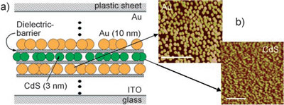
| Multilayer structure of an electrooptical device. a) Schematic representation of the tactile device showing the nanoparticle monolayers spaced by the organic dielectric layers that are made of four monolayers each of PSS and PAH. b) AFM topography image after subsequent deposition of the first gold (Au) layer and the first CdS layer. Scale bar: 100 nm. (Reprinted with permission from Wiley) | |
| "A five nanoparticle monolayer structure separated by dielectric layers has been constructed on a transparent indium-tin-oxide (ITO) electrode by using the layer-by-layer self-assembly technique. The dielectric layer is approximately 5–6 nm thick film composed of a total of four alternating monolayers of poly(allylamine hydrochloride) (PAH) and poly(styrene sulfonate) (PSS). The nanoparticles are well below the percolation threshold in thein-plane direction and, therefore, are not conducting; while the film is conducting in the direction perpendicular to the plane because the electrons can tunnel through the dielectric barrier. Electric current flows through the film and the CdS nanoparticles emit visible light at a wavelength of 580 nm (the electroluminescence light). The application of a load to the top of the Au/plastic electrode causes the dielectric layer to become compressed and the particles to get closer together, thus causing an increase in both the local current density and the electroluminescent light. The device has a resolution higher than 20 µm." | |
| Instead of measuring the electroluminescent light, the stress distribution can be obtained by measuring the local current density distribution in a configuration similar to a liquid-crystal display. Thus, a resolution of 40 µm, comparable to a human finger, can be achieved with this electrical device with no optical components. | |
 By
Michael
Berger
– Michael is author of three books by the Royal Society of Chemistry:
Nano-Society: Pushing the Boundaries of Technology,
Nanotechnology: The Future is Tiny, and
Nanoengineering: The Skills and Tools Making Technology Invisible
Copyright ©
Nanowerk LLC
By
Michael
Berger
– Michael is author of three books by the Royal Society of Chemistry:
Nano-Society: Pushing the Boundaries of Technology,
Nanotechnology: The Future is Tiny, and
Nanoengineering: The Skills and Tools Making Technology Invisible
Copyright ©
Nanowerk LLC
|
Become a Spotlight guest author! Join our large and growing group of guest contributors. Have you just published a scientific paper or have other exciting developments to share with the nanotechnology community? Here is how to publish on nanowerk.com.